
A English
Junction Transistor Questions in English
Class 12 Physics · Semiconductor Electronics · Junction Transistor
399+
Questions
English
Language
100%
With Solutions
Showing 44 of 399 questions in English
1
EasyMCQ
When $NPN$ transistor is used as an amplifier,
A
Electrons move from base to collector
B
Holes move from emitter to base
C
Electrons move from collector to base
D
Holes move from base to emitter
Solution
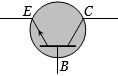
(A) In an $NPN$ transistor,the emitter is $N-$type,the base is $P-$type,and the collector is $N-$type. When used as an amplifier,the emitter-base junction is forward-biased and the collector-base junction is reverse-biased. Electrons,being the majority charge carriers in the $N-$type emitter,are injected into the base. Due to the thin base region,most of these electrons diffuse through the base and are collected by the collector. Thus,electrons move from the emitter to the base and then from the base to the collector.
0 likes
View Solution2
MediumMCQ
The phase difference between input and output voltages of a $CE$ (common emitter) amplifier circuit is........$^o$.
A
$0$
B
$90$
C
$180$
D
$270$
Solution
(C) In a common emitter $(CE)$ transistor amplifier,the input signal is applied between the base and emitter,and the output is taken across the collector and emitter.
When the input signal voltage increases,the base current increases,which in turn increases the collector current.
Due to the voltage drop across the load resistor in the collector circuit,the output voltage decreases.
Conversely,when the input signal voltage decreases,the collector current decreases,leading to an increase in the output voltage.
This inverse relationship between the input and output signals results in a phase shift of $\pi$ radians,which is equivalent to $180^o$.
0 likes
View Solution3
MediumMCQ
An oscillator is nothing but an amplifier with
A
Positive feedback
B
Large gain
C
No feedback
D
Negative feedback
Solution
(A) An oscillator is a circuit that produces a continuous,repeated,alternating waveform without any input signal.
It functions as an amplifier with positive feedback.
In this configuration,a portion of the output signal is fed back to the input in phase with the original signal.
This positive feedback reinforces the input,allowing the circuit to sustain oscillations indefinitely,provided the Barkhausen criterion (loop gain $A\beta = 1$ and phase shift of $360^{\circ}$ or $0^{\circ}$) is satisfied.
0 likes
View Solution4
EasyMCQ
The emitter-base junction of a transistor is …… biased while the collector-base junction is ……. biased.
A
Reverse,forward
B
Reverse,reverse
C
Forward,forward
D
Forward,reverse
Solution
(D) In a standard transistor configuration (such as the active region used for amplification),the emitter-base junction is forward-biased to allow charge carriers to flow from the emitter into the base.
Conversely,the collector-base junction is reverse-biased to collect the charge carriers that have crossed the base region.
Therefore,the correct configuration is forward-biased for the emitter-base junction and reverse-biased for the collector-base junction.
Conversely,the collector-base junction is reverse-biased to collect the charge carriers that have crossed the base region.
Therefore,the correct configuration is forward-biased for the emitter-base junction and reverse-biased for the collector-base junction.
0 likes
View Solution5
MediumMCQ
In an $NPN$ transistor,the collector current is $24 \, mA$. If $80\%$ of electrons reach the collector,its base current in $mA$ is:
A
$36$
B
$26$
C
$16$
D
$6$
Solution
(D) Given that the collector current $i_c = 24 \, mA$.
Since $80\%$ of the electrons emitted from the emitter reach the collector,we have the relation: $i_c = 0.80 \times i_e$.
Substituting the value of $i_c$: $24 = 0.80 \times i_e$.
Solving for the emitter current: $i_e = \frac{24}{0.80} = 30 \, mA$.
Using the Kirchhoff's current law for a transistor: $i_e = i_b + i_c$.
Rearranging to find the base current: $i_b = i_e - i_c$.
Substituting the known values: $i_b = 30 \, mA - 24 \, mA = 6 \, mA$.
Thus,the base current is $6 \, mA$.
0 likes
View Solution6
MediumMCQ
$A$ $NPN$ transistor conducts when
A
Both collector and emitter are positive with respect to the base
B
Collector is positive and emitter is negative with respect to the base
C
Collector is positive and emitter is at same potential as the base
D
Both collector and emitter are negative with respect to the base
Solution
(B) For an $NPN$ transistor to conduct (operate in the active region),the emitter-base junction must be forward-biased and the collector-base junction must be reverse-biased.
In an $NPN$ transistor,the base is $P$-type and the emitter and collector are $N$-type.
$1$. To forward-bias the emitter-base junction,the $N$-type emitter must be at a lower potential than the $P$-type base (i.e.,emitter is negative with respect to the base).
$2$. To reverse-bias the collector-base junction,the $N$-type collector must be at a higher potential than the $P$-type base (i.e.,collector is positive with respect to the base).
Therefore,the transistor conducts when the collector is positive and the emitter is negative with respect to the base.
0 likes
View Solution7
EasyMCQ
In the case of constants $\alpha$ and $\beta$ of a transistor:
A
$\alpha = \beta$
B
$\alpha < 1, \beta > 1$
C
$\alpha \beta = 1$
D
$\beta > 1, \alpha < 1$
Solution
(D) For a transistor,$\alpha$ (common-base current gain) is defined as the ratio of collector current $(I_C)$ to emitter current $(I_E)$,i.e.,$\alpha = \frac{I_C}{I_E}$. Since $I_E = I_C + I_B$,it follows that $I_C < I_E$,so $\alpha < 1$.
$\beta$ (common-emitter current gain) is defined as the ratio of collector current $(I_C)$ to base current $(I_B)$,i.e.,$\beta = \frac{I_C}{I_B}$. Since the base current $I_B$ is very small compared to the collector current $I_C$,$\beta$ is typically much greater than $1$.
Therefore,the correct relationship is $\alpha < 1$ and $\beta > 1$.
0 likes
View Solution8
EasyMCQ
Which of the following statements is true regarding transistor configurations?
A
Common base transistor is commonly used because current gain is maximum.
B
Common emitter is commonly used because current gain is maximum.
C
Common collector is commonly used because current gain is maximum.
D
Common emitter is the least used transistor.
Solution
(B) In a transistor, the common emitter $(CE)$ configuration is the most widely used because it provides both high current gain $(\beta)$ and high voltage gain, resulting in a high power gain.
In the common base $(CB)$ configuration, the current gain $(\alpha)$ is < $1$.
In the common collector $(CC)$ configuration, the current gain is high, but the voltage gain is < $1$.
Therefore, the common emitter configuration is preferred for amplification purposes.
In the common base $(CB)$ configuration, the current gain $(\alpha)$ is < $1$.
In the common collector $(CC)$ configuration, the current gain is high, but the voltage gain is < $1$.
Therefore, the common emitter configuration is preferred for amplification purposes.
0 likes
View Solution9
EasyMCQ
If $\alpha = 0.98$ and the current through the emitter $i_e = 20 \, mA$,the value of $\beta$ is
A
$4.9$
B
$49$
C
$96$
D
$9.6$
Solution
(B) The relationship between the common-base current gain $\alpha$ and the common-emitter current gain $\beta$ is given by the formula:
$\beta = \frac{\alpha}{1 - \alpha}$
Given $\alpha = 0.98$,we substitute the value into the formula:
$\beta = \frac{0.98}{1 - 0.98}$
$\beta = \frac{0.98}{0.02}$
$\beta = 49$
Thus,the value of $\beta$ is $49$.
$\beta = \frac{\alpha}{1 - \alpha}$
Given $\alpha = 0.98$,we substitute the value into the formula:
$\beta = \frac{0.98}{1 - 0.98}$
$\beta = \frac{0.98}{0.02}$
$\beta = 49$
Thus,the value of $\beta$ is $49$.
0 likes
View Solution10
MediumMCQ
For a common base configuration of a $PNP$ transistor,$\frac{I_C}{I_E} = 0.96$. Then,the maximum current gain in common emitter configuration will be:
A
$12$
B
$24$
C
$6$
D
$5$
Solution
(B) In a common base configuration,the current gain $\alpha$ is defined as the ratio of collector current $I_C$ to emitter current $I_E$.
Given: $\alpha = \frac{I_C}{I_E} = 0.96$.
The current gain in common emitter configuration,denoted by $\beta$,is related to $\alpha$ by the formula:
$\beta = \frac{\alpha}{1 - \alpha}$.
Substituting the given value:
$\beta = \frac{0.96}{1 - 0.96} = \frac{0.96}{0.04}$.
$\beta = 24$.
Therefore,the maximum current gain in common emitter configuration is $24$.
0 likes
View Solution11
MediumMCQ
In a $PNP$ transistor working as a common-base amplifier,current gain is $0.96$ and emitter current is $7.2 \, mA$. The base current is.....$mA$
A
$0.4$
B
$0.2$
C
$0.29$
D
$0.35$
Solution
(C) Given: Current gain $\alpha = 0.96$ and emitter current $I_e = 7.2 \, mA$.
In a common-base configuration,the current gain $\alpha$ is defined as $\alpha = \frac{I_c}{I_e}$.
Therefore,the collector current $I_c = \alpha \times I_e = 0.96 \times 7.2 \, mA = 6.912 \, mA$.
According to Kirchhoff's current law for a transistor,$I_e = I_c + I_b$.
Thus,the base current $I_b = I_e - I_c$.
$I_b = 7.2 \, mA - 6.912 \, mA = 0.288 \, mA$.
Rounding to two decimal places,$I_b \approx 0.29 \, mA$.
0 likes
View Solution12
EasyMCQ
If ${l_1}, {l_2}, {l_3}$ are the lengths of the emitter,base,and collector of a transistor,respectively,then:
A
${l_1} = {l_2} = {l_3}$
B
${l_3} < {l_2} > {l_1}$
C
${l_3} < {l_1} < {l_2}$
D
${l_3} > {l_1} > {l_2}$
Solution
(D) In a transistor,the collector is designed to collect the majority of charge carriers coming from the emitter. This process generates significant heat,so the collector is made with the largest surface area to dissipate this heat effectively.
The base is the middle region,which is made very thin and lightly doped to allow charge carriers to pass from the emitter to the collector with minimal recombination.
The emitter is moderately sized and heavily doped to supply charge carriers.
Comparing the sizes: The collector $(l_3)$ is the largest,the base $(l_2)$ is the smallest,and the emitter $(l_1)$ is of intermediate size.
Therefore,the correct relation is ${l_3} > {l_1} > {l_2}$.
0 likes
View Solution13
MediumMCQ
In an $NPN$ transistor circuit,the collector current is $10 \,mA$. If $90\%$ of the electrons emitted reach the collector,the emitter current $(i_E)$ and base current $(i_B)$ are given by
A
$i_E = -1 \,mA, i_B = 9 \,mA$
B
$i_E = 9 \,mA, i_B = -1 \,mA$
C
$i_E = 1 \,mA, i_B = 11 \,mA$
D
$i_E = 11 \,mA, i_B = 1 \,mA$
Solution
(D) Given that the collector current $i_C = 10 \,mA$.
Since $90\%$ of the electrons emitted from the emitter reach the collector,we have the relation $i_C = 0.90 \times i_E$.
Substituting the value of $i_C$,we get $10 = 0.90 \times i_E$.
Therefore,$i_E = \frac{10}{0.9} \approx 11.11 \,mA$. Rounding to the nearest integer as per the options,$i_E = 11 \,mA$.
Using the Kirchhoff's current law for a transistor,$i_E = i_B + i_C$.
Substituting the values,$11 = i_B + 10$.
Thus,$i_B = 11 - 10 = 1 \,mA$.
0 likes
View Solution14
MediumMCQ
In a common emitter transistor,the current gain is $80$. What is the change in collector current,when the change in base current is $250 \ \mu A$?
A
$80 \times 250 \ \mu A$
B
$(250 - 80) \ \mu A$
C
$(250 + 80) \ \mu A$
D
$250 / 80 \ \mu A$
Solution
(A) The current gain $\beta$ in a common emitter configuration is defined as the ratio of the change in collector current $\Delta I_C$ to the change in base current $\Delta I_B$.
Formula: $\beta = \frac{\Delta I_C}{\Delta I_B}$
Given: $\beta = 80$ and $\Delta I_B = 250 \ \mu A$.
To find the change in collector current $\Delta I_C$,we rearrange the formula:
$\Delta I_C = \beta \times \Delta I_B$
$\Delta I_C = 80 \times 250 \ \mu A$
Therefore,the change in collector current is $80 \times 250 \ \mu A$.
0 likes
View Solution15
EasyMCQ
Which region is the least doped in a transistor?
A
Either emitter or collector
B
Base
C
Emitter
D
Collector
Solution
(B) In a bipolar junction transistor,the emitter is heavily doped to provide a large number of charge carriers. The collector is moderately doped to handle the power dissipation. The base is made very thin and is lightly (least) doped to ensure that most of the charge carriers injected from the emitter pass through to the collector without recombining in the base. Therefore,the base is the least doped region.
0 likes
View Solution16
EasyMCQ
The transistors provide good power amplification when they are used in
A
Common collector configuration
B
Common emitter configuration
C
Common base configuration
D
None of these
Solution
(B) In a transistor, the power gain is defined as the product of current gain $(\beta)$ and voltage gain $(A_v)$.
In a $Common \text{ } Emitter$ $(CE)$ configuration, both the current gain $(\beta)$ and the voltage gain are significantly greater than $1$.
Since the $CE$ configuration provides both high current gain and high voltage gain, it results in a high power gain.
Therefore, transistors provide good power amplification when they are used in the $Common \text{ } Emitter$ configuration.
0 likes
View Solution17
MediumMCQ
The transfer ratio of a transistor is $50$. The input resistance of the transistor when used in the common-emitter configuration is $1 \; k\Omega$. The peak value of the collector current for an $A.C.$ input voltage of $0.01 \; V$ peak is:
A
$100 \; \mu A$
B
$0.01 \; mA$
C
$0.25 \; mA$
D
$500 \; \mu A$
Solution
(D) Given: Transfer ratio (current gain) $\beta = 50$,Input resistance $R_i = 1 \; k\Omega = 1000 \; \Omega$,and Peak input voltage $V_i = 0.01 \; V$.
First,calculate the peak input current $i_b$ using Ohm's law: $i_b = \frac{V_i}{R_i} = \frac{0.01 \; V}{1000 \; \Omega} = 10^{-5} \; A$.
The relationship between collector current $i_c$ and base current $i_b$ is given by $\beta = \frac{i_c}{i_b}$.
Therefore,the peak collector current is $i_c = \beta \times i_b = 50 \times 10^{-5} \; A = 500 \times 10^{-6} \; A = 500 \; \mu A$.
0 likes
View Solution18
EasyMCQ
For a transistor,the parameter $\beta = 99$. The value of the parameter $\alpha$ is
A
$0.9$
B
$0.99$
C
$1$
D
$9$
Solution
(B) The relationship between the common-emitter current gain $\beta$ and the common-base current gain $\alpha$ is given by the formula: $\alpha = \frac{\beta}{1 + \beta}$.
Given $\beta = 99$.
Substituting the value into the formula:
$\alpha = \frac{99}{1 + 99} = \frac{99}{100} = 0.99$.
Therefore,the value of $\alpha$ is $0.99$.
Given $\beta = 99$.
Substituting the value into the formula:
$\alpha = \frac{99}{1 + 99} = \frac{99}{100} = 0.99$.
Therefore,the value of $\alpha$ is $0.99$.
0 likes
View Solution19
MediumMCQ
$A$ transistor is used in common emitter mode as an amplifier. Then:
A
The base-emitter junction is forward biased.
B
The base-emitter junction is reverse biased.
C
The input signal is connected in series with the voltage applied to the base-emitter junction.
D
Both $(a)$ and $(c)$ are correct.
Solution
(D) In a common emitter $(CE)$ amplifier configuration,the transistor must be operated in the active region.
For the active region,the base-emitter junction must be forward-biased,and the collector-base junction must be reverse-biased.
Therefore,statement $(a)$ is correct.
Furthermore,in a $CE$ amplifier,the input signal is applied to the base-emitter circuit,which is in series with the $DC$ bias voltage applied to the base-emitter junction.
Therefore,statement $(c)$ is also correct.
Thus,both $(a)$ and $(c)$ are correct.
0 likes
View Solution20
EasyMCQ
In a $PNP$ transistor,the base is the $N$-region. Its width relative to the $P$-region is
A
Smaller
B
Larger
C
Same
D
Not related
Solution
(A) In a transistor,the base region is intentionally made very thin and lightly doped compared to the emitter and collector regions.
This design ensures that the majority of charge carriers injected from the emitter into the base can diffuse through the base and reach the collector region before they can recombine.
Therefore,in a $PNP$ transistor,the width of the $N$-type base is much smaller than the width of the $P$-type emitter and collector regions.
0 likes
View Solution21
MediumMCQ
$A$ common emitter amplifier is designed with an $NPN$ transistor $(\alpha = 0.99)$. The input impedance is $1 \ k\Omega$ and the load resistance is $10 \ k\Omega$. The voltage gain will be:
A
$9.9$
B
$99$
C
$990$
D
$9900$
Solution
(C) The voltage gain $(A_v)$ of a common emitter amplifier is given by the product of the current gain $(\beta)$ and the resistance gain.
First,calculate the current gain $\beta$ using the relation $\beta = \frac{\alpha}{1 - \alpha}$:
$\beta = \frac{0.99}{1 - 0.99} = \frac{0.99}{0.01} = 99$.
Next,calculate the resistance gain,which is the ratio of the load resistance $(R_L)$ to the input impedance $(R_i)$:
Resistance gain $= \frac{R_L}{R_i} = \frac{10 \ k\Omega}{1 \ k\Omega} = 10$.
Finally,calculate the voltage gain:
$A_v = \beta \times \text{Resistance gain} = 99 \times 10 = 990$.
0 likes
View Solution22
EasyMCQ
A
$NPN$ transistor
B
$PNP$ transistor
C
Forward biased $PN$ junction diode
D
Reverse biased $NP$ junction diode
Solution
0 likes
View Solution23
MediumMCQ
An $NPN$ transistor circuit is arranged as shown in the figure. It is:
A
$A$ common base amplifier circuit
B
$A$ common emitter amplifier circuit
C
$A$ common collector amplifier circuit
D
Neither of the above
Solution
(B) In the given circuit diagram,the emitter terminal of the $NPN$ transistor is connected to the ground,which is common to both the input circuit (between base and emitter) and the output circuit (between collector and emitter). Since the emitter is the common terminal between the input and output,this configuration is known as a common emitter amplifier circuit.
0 likes
View Solution24
EasyMCQ
The part of a transistor which is heavily doped to produce a large number of majority carriers is
A
Base
B
Emitter
C
Collector
D
Can be any of the above three
Solution
(B) In a transistor,the $Emitter$ is the section that is heavily doped. The purpose of heavy doping is to provide a large number of majority charge carriers,which are then injected into the $Base$ region. The $Base$ is lightly doped and thin,while the $Collector$ is moderately doped. Therefore,the correct option is $B$.
0 likes
View Solution25
MediumMCQ
For a transistor,the current amplification factor is $\alpha = 0.8$. The transistor is connected in a common emitter configuration. The change in the collector current when the base current changes by $6 \, mA$ is.....$mA$.
A
$6$
B
$4.8$
C
$24$
D
$8$
Solution
(C) Given,current amplification factor $\alpha = 0.8$.
For a common emitter configuration,the current gain $\beta$ is related to $\alpha$ by the formula $\beta = \frac{\alpha}{1 - \alpha}$.
Substituting the value of $\alpha$:
$\beta = \frac{0.8}{1 - 0.8} = \frac{0.8}{0.2} = 4$.
We know that the current gain $\beta$ is defined as the ratio of the change in collector current $\Delta I_c$ to the change in base current $\Delta I_b$:
$\beta = \frac{\Delta I_c}{\Delta I_b}$.
Given $\Delta I_b = 6 \, mA$,we can calculate $\Delta I_c$ as:
$\Delta I_c = \beta \times \Delta I_b = 4 \times 6 \, mA = 24 \, mA$.
Therefore,the change in collector current is $24 \, mA$.
0 likes
View Solution26
MediumMCQ
In a common base amplifier circuit,calculate the change in base current if the change in emitter current is $2\, mA$ and $\alpha = 0.98$.
A
$0.04$
B
$1.96$
C
$0.98$
D
$2$
Solution
(A) In a transistor,the relationship between currents is given by $\Delta i_e = \Delta i_c + \Delta i_b$.
Given $\alpha = \frac{\Delta i_c}{\Delta i_e} = 0.98$ and $\Delta i_e = 2\, mA$.
First,calculate the change in collector current: $\Delta i_c = \alpha \times \Delta i_e = 0.98 \times 2 = 1.96\, mA$.
Now,calculate the change in base current: $\Delta i_b = \Delta i_e - \Delta i_c$.
$\Delta i_b = 2\, mA - 1.96\, mA = 0.04\, mA$.
0 likes
View Solution27
EasyMCQ
In the case of $NPN$ transistors,the collector current is always less than the emitter current because:
A
Collector side is reverse biased and emitter side is forward biased
B
After electrons are lost in the base,only the remaining ones reach the collector
C
Collector side is forward biased and emitter side is reverse biased
D
Collector being reverse biased attracts fewer electrons
Solution
(B) In an $NPN$ transistor,the emitter current $(I_E)$ is the sum of the base current $(I_B)$ and the collector current $(I_C)$,expressed as $I_E = I_B + I_C$.
Since a small fraction of electrons injected from the emitter recombine with holes in the base region,the base current $(I_B)$ is non-zero.
Therefore,the collector current is given by $I_C = I_E - I_B$.
Because $I_B > 0$,it follows that $I_C < I_E$.
Since a small fraction of electrons injected from the emitter recombine with holes in the base region,the base current $(I_B)$ is non-zero.
Therefore,the collector current is given by $I_C = I_E - I_B$.
Because $I_B > 0$,it follows that $I_C < I_E$.
0 likes
View Solution28
MediumMCQ
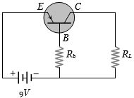
In the transistor circuit shown,the base current is $35 \mu A$. The value of the resistor $R_b$ is......$ k \Omega$.
A
$123.5$
B
$257$
C
$380.05$
D
None of these
Solution
(B) From the given circuit diagram,the base-emitter loop consists of the $9 \text{ V}$ battery and the base resistor $R_b$.
Applying Kirchhoff's voltage law to the base-emitter loop (assuming the base-emitter voltage $V_{BE} \approx 0 \text{ V}$ for an ideal transistor or that the $9 \text{ V}$ is applied directly across $R_b$):
$V_b = i_b \times R_b$
Given $V_b = 9 \text{ V}$ and $i_b = 35 \mu A = 35 \times 10^{-6} \text{ A}$.
$R_b = \frac{V_b}{i_b} = \frac{9}{35 \times 10^{-6}} \Omega$
$R_b = \frac{9}{35} \times 10^6 \Omega \approx 0.25714 \times 10^6 \Omega$
$R_b \approx 257.14 \times 10^3 \Omega = 257.14 \text{ k}\Omega$.
Rounding to the nearest integer,we get $257 \text{ k}\Omega$.
0 likes
View Solution29
MediumMCQ
In a transistor,a change of $8.0\, mA$ in the emitter current produces a change of $7.8\, mA$ in the collector current. What change in the base current is necessary to produce the same change in the collector current? (in $\mu A$)
A
$50$
B
$100$
C
$150$
D
$200$
Solution
(D) For a transistor,the relationship between the changes in currents is given by the equation: $\Delta I_e = \Delta I_c + \Delta I_b$.
Given: $\Delta I_e = 8.0\, mA$ and $\Delta I_c = 7.8\, mA$.
Substituting these values into the equation: $8.0\, mA = 7.8\, mA + \Delta I_b$.
Solving for the change in base current: $\Delta I_b = 8.0\, mA - 7.8\, mA = 0.2\, mA$.
Converting the result to microamperes $(\mu A)$: $0.2\, mA = 0.2 \times 10^3\, \mu A = 200\, \mu A$.
0 likes
View Solution30
EasyMCQ
In a transistor configuration,the $\beta$-parameter is defined as:
A
$\frac{I_b}{I_c}$
B
$\frac{I_c}{I_b}$
C
$\frac{I_c}{I_e}$
D
$\frac{I_e}{I_c}$
Solution
(B) In a common-emitter transistor configuration,the current gain $\beta$ is defined as the ratio of the collector current $(I_c)$ to the base current $(I_b)$.
Mathematically,$\beta = \frac{I_c}{I_b}$.
Therefore,the correct option is $B$.
Mathematically,$\beta = \frac{I_c}{I_b}$.
Therefore,the correct option is $B$.
0 likes
View Solution31
EasyMCQ
Which of these is a unipolar transistor?
A
Point contact transistor
B
Field effect transistor
C
$PNP$ transistor
D
None of these
Solution
(B) unipolar transistor is a device in which the current conduction is due to only one type of charge carrier (either electrons or holes).
$FET$ (Field Effect Transistor) is a unipolar device because the current in it is carried by only one type of majority charge carrier.
In contrast,$PNP$ and $NPN$ transistors are bipolar junction transistors $(BJT)$ because their current conduction involves both electrons and holes.
$FET$ (Field Effect Transistor) is a unipolar device because the current in it is carried by only one type of majority charge carrier.
In contrast,$PNP$ and $NPN$ transistors are bipolar junction transistors $(BJT)$ because their current conduction involves both electrons and holes.
0 likes
View Solution32
MediumMCQ
For a transistor,in a common emitter arrangement,the alternating current gain $\beta$ is given by
A
$\beta = \left( \frac{\Delta I_C}{\Delta I_B} \right)_{V_{CE}}$
B
$\beta = \left( \frac{\Delta I_B}{\Delta I_C} \right)_{V_{CE}}$
C
$\beta = \left( \frac{\Delta I_C}{\Delta I_E} \right)_{V_{CE}}$
D
$\beta = \left( \frac{\Delta I_E}{\Delta I_C} \right)_{V_{CE}}$
Solution
(A) In a common emitter configuration,the alternating current gain $\beta$ (also known as the forward current gain) is defined as the ratio of the change in collector current $\Delta I_C$ to the change in base current $\Delta I_B$,while keeping the collector-emitter voltage $V_{CE}$ constant.
Mathematically,this is expressed as: $\beta = \left( \frac{\Delta I_C}{\Delta I_B} \right)_{V_{CE}}$.
Since it is a ratio of two currents,$\beta$ is a dimensionless quantity. $A$ small change in the base current results in a significantly larger change in the collector current,which is the fundamental principle behind transistor amplification.
0 likes
View Solution33
MediumMCQ
The relation between $\alpha$ and $\beta$ parameters of current gains for a transistor is given by:
A
$\alpha = \frac{\beta}{1 - \beta}$
B
$\alpha = \frac{\beta}{1 + \beta}$
C
$\alpha = \frac{1 - \beta}{\beta}$
D
$\alpha = \frac{1 + \beta}{\beta}$
Solution
(B) In a transistor,the emitter current $i_e$ is the sum of the base current $i_b$ and the collector current $i_c$:
$i_e = i_b + i_c$
Dividing both sides by $i_c$:
$\frac{i_e}{i_c} = \frac{i_b}{i_c} + 1$
We know that $\alpha = \frac{i_c}{i_e}$ (so $\frac{i_e}{i_c} = \frac{1}{\alpha}$) and $\beta = \frac{i_c}{i_b}$ (so $\frac{i_b}{i_c} = \frac{1}{\beta}$).
Substituting these values:
$\frac{1}{\alpha} = \frac{1}{\beta} + 1$
$\frac{1}{\alpha} = \frac{1 + \beta}{\beta}$
Therefore,$\alpha = \frac{\beta}{1 + \beta}$.
0 likes
View Solution34
MediumMCQ
When an $NPN$ transistor is used as an amplifier,which of the following occurs?
A
Electrons move from base to emitter.
B
Electrons move from emitter to base.
C
Holes move from emitter to base.
D
Holes move from base to emitter.
Solution
(B) In an $NPN$ transistor,the emitter is heavily doped with electrons. When the emitter-base junction is forward-biased,the potential barrier is lowered. This allows the majority charge carriers (electrons) in the emitter to be injected into the base region. Therefore,electrons move from the emitter to the base.
0 likes
View Solution35
MediumMCQ
In the $CB$ mode of a transistor, when the collector voltage is changed by $0.5\,V$, the collector current changes by $0.05\,mA$. The output resistance will be....$k\Omega$.
A
$10$
B
$20$
C
$5$
D
$2.5$
Solution
(A) The output resistance $(R_{out})$ in $CB$ mode is defined as the ratio of the change in collector voltage $(\Delta V_C)$ to the change in collector current $(\Delta I_C)$ while keeping the emitter current constant.
Given: $\Delta V_C = 0.5\,V$ and $\Delta I_C = 0.05\,mA = 0.05 \times 10^{-3}\,A$.
Using the formula: $R_{out} = \frac{\Delta V_C}{\Delta I_C}$.
Substituting the values: $R_{out} = \frac{0.5}{0.05 \times 10^{-3}} = \frac{0.5}{5 \times 10^{-5}} = 0.1 \times 10^5 = 10^4\,\Omega$.
Since $10^4\,\Omega = 10 \times 10^3\,\Omega = 10\,k\Omega$.
Therefore, the output resistance is $10\,k\Omega$.
0 likes
View Solution36
MediumMCQ
While a collector to emitter voltage is constant in a transistor,the collector current changes by $8.2 \, mA$ when the emitter current changes by $8.3 \, mA$. The value of forward current gain $h_{fe}$ is
A
$82$
B
$83$
C
$8.2$
D
$8.3$
Solution
(A) In a transistor,the emitter current $I_e$ is the sum of collector current $I_c$ and base current $I_b$,so $\Delta I_e = \Delta I_c + \Delta I_b$.
Given: $\Delta I_c = 8.2 \, mA$ and $\Delta I_e = 8.3 \, mA$.
First,calculate the change in base current: $\Delta I_b = \Delta I_e - \Delta I_c = 8.3 \, mA - 8.2 \, mA = 0.1 \, mA$.
The forward current gain $h_{fe}$ (also denoted as $\beta$) is defined as the ratio of change in collector current to the change in base current at a constant collector-emitter voltage: $h_{fe} = \frac{\Delta I_c}{\Delta I_b}$.
Substituting the values: $h_{fe} = \frac{8.2 \, mA}{0.1 \, mA} = 82$.
0 likes
View Solution37
MediumMCQ
Consider an $NPN$ transistor amplifier in common-emitter configuration. The current gain of the transistor is $100$. If the collector current changes by $1\, mA$,what will be the change in emitter current in $mA$?
A
$1.1$
B
$1.01$
C
$0.01$
D
$10$
Solution
(B) Given: Current gain $\beta = 100$,Change in collector current $\Delta I_c = 1\, mA$.
We know that the current gain in common-emitter configuration is defined as $\beta = \frac{\Delta I_c}{\Delta I_b}$.
Therefore,the change in base current is $\Delta I_b = \frac{\Delta I_c}{\beta} = \frac{1\, mA}{100} = 0.01\, mA$.
The relationship between emitter,collector,and base currents is $\Delta I_e = \Delta I_c + \Delta I_b$.
Substituting the values,we get $\Delta I_e = 1\, mA + 0.01\, mA = 1.01\, mA$.
Thus,the change in emitter current is $1.01\, mA$.
0 likes
View Solution38
EasyMCQ
In a common base amplifier,the phase difference between the input signal voltage and the output voltage is
A
$0$
B
$\pi /4$
C
$\pi /2$
D
$\pi$
Solution
(A) In a common base $(CB)$ amplifier configuration,the input signal is applied between the emitter and the base,and the output is taken between the collector and the base.
Since the base is common to both the input and output circuits,the input voltage and output voltage signals are in the same phase.
Therefore,the phase difference between the input signal voltage and the output voltage is $0$.
Since the base is common to both the input and output circuits,the input voltage and output voltage signals are in the same phase.
Therefore,the phase difference between the input signal voltage and the output voltage is $0$.
0 likes
View Solution39
EasyMCQ
In an $NPN$ transistor,the collector current is $10\, mA$. If $90\%$ of the electrons emitted reach the collector,then:
A
Emitter current will be $9\, mA$
B
Emitter current will be $11.1\, mA$
C
Base current will be $0.1\, mA$
D
Base current will be $0.01\, mA$
Solution
(B) Given that the collector current $I_C = 10\, mA$.
Since $90\%$ of the electrons emitted reach the collector,the collector current is $90\%$ of the emitter current $(I_E)$.
Therefore,$I_C = 0.90 \times I_E$.
Substituting the value of $I_C$: $10\, mA = 0.90 \times I_E$.
Solving for $I_E$: $I_E = \frac{10}{0.90} = 11.11\, mA$.
Using the relation $I_E = I_B + I_C$,we can find the base current $I_B$:
$I_B = I_E - I_C = 11.11\, mA - 10\, mA = 1.11\, mA$.
Comparing this with the given options,the correct statement is that the emitter current is $11.1\, mA$.
0 likes
View Solution40
MediumMCQ
In a transistor in $CE$ configuration,the ratio of power gain to voltage gain is
A
$\alpha$
B
$\beta / \alpha$
C
$\beta \alpha$
D
$\beta$
Solution
(D) For a transistor in $CE$ configuration,the voltage gain $(A_v)$ is given by $A_v = \beta \times \frac{R_L}{R_i}$,where $\beta$ is the current gain,$R_L$ is the load resistance,and $R_i$ is the input resistance.
The power gain $(A_p)$ is given by $A_p = \beta^2 \times \frac{R_L}{R_i}$.
Therefore,the ratio of power gain to voltage gain is:
$\frac{A_p}{A_v} = \frac{\beta^2 \times (R_L / R_i)}{\beta \times (R_L / R_i)} = \beta$.
Thus,the correct option is $D$.
The power gain $(A_p)$ is given by $A_p = \beta^2 \times \frac{R_L}{R_i}$.
Therefore,the ratio of power gain to voltage gain is:
$\frac{A_p}{A_v} = \frac{\beta^2 \times (R_L / R_i)}{\beta \times (R_L / R_i)} = \beta$.
Thus,the correct option is $D$.
0 likes
View Solution41
MediumMCQ
In the study of a transistor as an amplifier,if $\alpha = \frac{I_{C}}{I_{E}}$ and $\beta = \frac{I_{C}}{I_{B}}$,where $I_{C}$,$I_{B}$,and $I_{E}$ are the collector,base,and emitter currents respectively,then:
A
$\beta = \frac{1 - \alpha}{\alpha}$
B
$\beta = \frac{\alpha}{1 - \alpha}$
C
$\beta = \frac{\alpha}{1 + \alpha}$
D
$\beta = \frac{1 + \alpha}{\alpha}$
Solution
(B) We know that the emitter current is the sum of the collector current and the base current:
$I_{E} = I_{C} + I_{B}$
Dividing both sides by $I_{C}$:
$\frac{I_{E}}{I_{C}} = 1 + \frac{I_{B}}{I_{C}}$
Since $\alpha = \frac{I_{C}}{I_{E}}$,it follows that $\frac{1}{\alpha} = \frac{I_{E}}{I_{C}}$.
Since $\beta = \frac{I_{C}}{I_{B}}$,it follows that $\frac{1}{\beta} = \frac{I_{B}}{I_{C}}$.
Substituting these into the equation:
$\frac{1}{\alpha} = 1 + \frac{1}{\beta}$
Rearranging to solve for $\frac{1}{\beta}$:
$\frac{1}{\beta} = \frac{1}{\alpha} - 1 = \frac{1 - \alpha}{\alpha}$
Therefore,$\beta = \frac{\alpha}{1 - \alpha}$.
0 likes
View Solution42
MediumMCQ
For a transistor amplifier in common emitter configuration with a load impedance of $1 \ k\Omega$ ($h_{fe} = 50$ and $h_{oe} = 25 \ \mu A/V$),the current gain is:
A
$-5.2$
B
$-15.7$
C
$-24.8$
D
$-48.78$
Solution
(D) In a common emitter configuration,the current gain $A_i$ is given by the formula:
$A_i = \frac{-h_{fe}}{1 + h_{oe} R_L}$
Given:
$h_{fe} = 50$
$h_{oe} = 25 \ \mu A/V = 25 \times 10^{-6} \ S$
$R_L = 1 \ k\Omega = 10^3 \ \Omega$
Substituting the values:
$A_i = \frac{-50}{1 + (25 \times 10^{-6}) \times 10^3}$
$A_i = \frac{-50}{1 + 0.025}$
$A_i = \frac{-50}{1.025}$
$A_i \approx -48.78$
0 likes
View Solution43
MediumMCQ
In the following common emitter configuration, an $NPN$ transistor with current gain $\beta = 100$ is used. The output voltage of the amplifier will be
A
$10 \, mV$
B
$0.1 \, V$
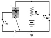
C
$1.0 \, V$
D
$10 \, V$
Solution
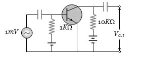
(C) Given: Input voltage $V_{in} = 1 \, mV = 10^{-3} \, V$, current gain $\beta = 100$, input resistance $R_{in} = 1 \, k\Omega = 10^3 \, \Omega$, and load resistance $R_L = 10 \, k\Omega = 10^4 \, \Omega$.
Voltage gain $A_v = \beta \times \frac{R_L}{R_{in}}$.
$A_v = 100 \times \frac{10 \, k\Omega}{1 \, k\Omega} = 100 \times 10 = 1000$.
Output voltage $V_{out} = A_v \times V_{in}$.
$V_{out} = 1000 \times 10^{-3} \, V = 1 \, V$.
Voltage gain $A_v = \beta \times \frac{R_L}{R_{in}}$.
$A_v = 100 \times \frac{10 \, k\Omega}{1 \, k\Omega} = 100 \times 10 = 1000$.
Output voltage $V_{out} = A_v \times V_{in}$.
$V_{out} = 1000 \times 10^{-3} \, V = 1 \, V$.
0 likes
View Solution44
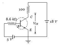
MediumMCQ
For the transistor circuit shown below,if $\beta = 100$ and the voltage drop between the emitter and base is $0.7 \, V$,then the value of $V_{CE}$ will be......$V$.
A
$10$
B
$5$
C
$13$
D
$0$
Solution
(C) $1$. Apply Kirchhoff's Voltage Law $(KVL)$ to the base-emitter loop:
$V_{BB} - I_B R_B - V_{BE} = 0$
$5 \, V - I_B (8.6 \, k\Omega) - 0.7 \, V = 0$
$I_B = \frac{5 - 0.7}{8.6 \times 10^3} = \frac{4.3}{8.6 \times 10^3} = 0.5 \times 10^{-3} \, A = 0.5 \, mA$.
$2$. Calculate the collector current $(I_C)$:
$I_C = \beta I_B = 100 \times 0.5 \, mA = 50 \, mA = 0.05 \, A$.
$3$. Apply $KVL$ to the collector-emitter loop:
$V_{CC} - I_C R_L - V_{CE} = 0$
$18 \, V - (0.05 \, A)(100 \, \Omega) - V_{CE} = 0$
$18 \, V - 5 \, V - V_{CE} = 0$
$V_{CE} = 13 \, V$.
0 likes
View SolutionSemiconductor Electronics — Junction Transistor · Frequently Asked Questions
1Are these Semiconductor Electronics questions useful for JEE and NEET?
Yes. All questions in this section are mapped to JEE Main and NEET exam patterns. Previous year questions from JEE Main, NEET, GUJCET and state-level exams are included with full solutions.
2Can I switch to Hindi or Gujarati for these questions?
Yes. Use the language tabs in the hero section or the sidebar to view the same questions and solutions in English, Hindi or Gujarati.
3How do I generate a question paper from this subtopic?
Use the Vedclass Exam Paper Generator — select the chapter and subtopic, set difficulty, and generate Sets A, B, C, D automatically. First 3 chapters of every subject are free.
Vedclass Products
For Students
Vedclass Test Series
Mock tests in real JEE/NEET style with performance analysis. 5-day free trial.
Start Free TrialFor Teachers
Exam Paper Generator
Generate Set A/B/C/D papers from this chapter in 2 minutes. 3 chapters free.
Try FreeFor Institutes
Online Exam Module
Live online exams with unlimited students, 360° analytics & white-label branding.
See DemoFor Teachers & Institutes
Generate a Semiconductor Electronics Exam Paper in 2 Minutes
Select subtopic & difficulty — Sets A, B, C, D auto-generated with No Repeat logic.
First 3 chapters of every subject are free — no payment required.