
A English
Light Emitting Diode (L.E.D), Photodiode, Solar Cell Questions in English
Class 12 Physics · Semiconductor Electronics · Light Emitting Diode (L.E.D), Photodiode, Solar Cell
118+
Questions
English
Language
100%
With Solutions
Showing 49 of 118 questions in English
1
EasyMCQ
The laptop PCs,modern electronic watches,and calculators use the following for display:
A
Single crystal
B
Poly crystal
C
Liquid crystal
D
Semiconductors
Solution
(C) Modern electronic devices such as laptop PCs,digital watches,and calculators utilize Liquid Crystal Displays $(LCDs)$.
Liquid crystals are a state of matter that has properties between those of conventional liquids and those of solid crystals.
They can be manipulated by electric fields to control the transmission of light,making them ideal for low-power display applications.
Liquid crystals are a state of matter that has properties between those of conventional liquids and those of solid crystals.
They can be manipulated by electric fields to control the transmission of light,making them ideal for low-power display applications.
0 likes
View Solution2
EasyMCQ
In a $PN$ junction photocell,the value of the photo-electromotive force produced by monochromatic light is proportional to
A
The voltage applied at the $PN$ junction
B
The barrier voltage at the $PN$ junction
C
The intensity of the light falling on the cell
D
The frequency of the light falling on the cell
Solution
(C) When monochromatic light with energy greater than the bandgap of the semiconductor falls on the $PN$ junction,it creates electron-hole pairs.
The number of electron-hole pairs generated is directly proportional to the number of incident photons.
Since the photo-electromotive force (photo-$EMF$) is generated due to the separation of these charge carriers by the junction's electric field,the magnitude of the photo-$EMF$ is directly proportional to the intensity of the incident light.
0 likes
View Solution3
EasyMCQ
The symbolic representation of a photodiode is:
A
B
C
D
Solution
(C) photodiode is a special type of $p-n$ junction diode that is sensitive to light. When it is illuminated by light radiations,electron-hole pairs are generated in the depletion region,which in turn produces an electric current. The symbol for a photodiode consists of a standard diode symbol with two arrows pointing towards the diode,indicating that light is incident on it. Therefore,option $C$ is the correct symbolic representation.
0 likes
View Solution4
MediumMCQ
$A$ photodetector is made from a semiconductor $In_{0.53}Ga_{0.47}As$ with $E_g = 0.73 \, eV$. What is the maximum wavelength,which it can detect in $nm$?
A
$1000$
B
$1703$
C
$500$
D
$173$
Solution
(B) The energy of the incident photon must be at least equal to the band gap energy $E_g$ of the semiconductor to excite an electron from the valence band to the conduction band.
Thus,the condition for detection is $h\nu \geq E_g$.
The maximum wavelength $\lambda_{max}$ corresponds to the minimum energy,which is equal to the band gap energy $E_g$.
$\lambda_{max} = \frac{hc}{E_g}$
Given $h = 6.63 \times 10^{-34} \, J \cdot s$,$c = 3 \times 10^8 \, m/s$,and $E_g = 0.73 \, eV = 0.73 \times 1.6 \times 10^{-19} \, J$.
$\lambda_{max} = \frac{6.63 \times 10^{-34} \times 3 \times 10^8}{0.73 \times 1.6 \times 10^{-19}} \, m$
$\lambda_{max} \approx 1.703 \times 10^{-6} \, m = 1703 \, nm$.
0 likes
View Solution5
EasyMCQ
$A$ photodetector is fabricated from a semiconductor with a band gap $E_g = 0.73 \, eV$. What is the maximum wavelength (in $nm$) it can detect?
A
$1000$
B
$1703$
C
$500$
D
$173$
Solution
(B) The energy of the incident photon must be at least equal to the band gap energy $E_g$ to excite an electron from the valence band to the conduction band.
Thus,$E = \frac{hc}{\lambda} = E_g$.
Rearranging for wavelength: $\lambda = \frac{hc}{E_g}$.
Given $h = 6.63 \times 10^{-34} \, J \cdot s$,$c = 3 \times 10^8 \, m/s$,and $E_g = 0.73 \, eV = 0.73 \times 1.6 \times 10^{-19} \, J$.
Substituting the values:
$\lambda = \frac{6.63 \times 10^{-34} \times 3 \times 10^8}{0.73 \times 1.6 \times 10^{-19}} \, m$.
$\lambda \approx 1.703 \times 10^{-6} \, m = 1703 \, nm$.
0 likes
View Solution6
EasyMCQ
In optical fiber communication, an $APD$ semiconductor is used for:
A
Converting sound waves into optical waves
B
Detecting the intensity of modulated signals
C
Converting optical signals into electrical signals
D
Converting electrical signals into optical signals
Solution
(C) An $APD$ stands for Avalanche Photodiode.
In an optical fiber communication system, the receiver end requires a device that can detect the incoming light pulses and convert them back into electrical signals.
An $APD$ is a highly sensitive semiconductor photodiode that uses the avalanche effect to provide gain, making it ideal for detecting weak optical signals and converting them into electrical signals.
Therefore, the correct function of an $APD$ is to convert optical signals into electrical signals.
0 likes
View Solution7
EasyMCQ
Which semiconductor device converts electrical energy into light?
A
Solar cell
B
Photodiode
C
Varactor diode
D
$LED$
Solution
(D) Light Emitting Diode $(LED)$ is a semiconductor $p-n$ junction device that emits light when an electric current passes through it in the forward-biased direction.
In an $LED$,the recombination of electrons and holes releases energy in the form of photons,thus converting electrical energy into light energy.
Conversely,a solar cell and a photodiode convert light energy into electrical energy.
In an $LED$,the recombination of electrons and holes releases energy in the form of photons,thus converting electrical energy into light energy.
Conversely,a solar cell and a photodiode convert light energy into electrical energy.
0 likes
View Solution8
EasyMCQ
Which of the following semiconductor devices requires a reverse bias to operate?
A
$LED$
B
Solar cell
C
Photodiode
D
Transistor
Solution
(C) $Photodiode$ is a $p-n$ junction diode that is specifically designed to operate under reverse bias conditions.
When light falls on the junction of a reverse-biased $Photodiode$,electron-hole pairs are generated,which increases the reverse saturation current.
$LEDs$ operate under forward bias,and solar cells operate without any external bias (photovoltaic mode).
When light falls on the junction of a reverse-biased $Photodiode$,electron-hole pairs are generated,which increases the reverse saturation current.
$LEDs$ operate under forward bias,and solar cells operate without any external bias (photovoltaic mode).
0 likes
View Solution9
EasyMCQ
The active area of a solar cell is $......$ so that the power obtained $......$.
A
small,increases
B
large,increases
C
large,decreases
D
small,decreases
Solution
(B) solar cell is a device that converts solar energy into electrical energy.
To generate a significant amount of electrical power,the solar cell must be able to capture as much incident sunlight as possible.
Since the power output is directly proportional to the area of the solar cell exposed to light,a larger active area allows for the absorption of more photons.
Therefore,the active area of a solar cell is made large so that the power obtained increases.
0 likes
View Solution10
MediumMCQ
The bandgap of the material of a photodiode is $2.0 \ eV$. What is the minimum frequency of radiation that this material can absorb?
A
$1 \times 10^{14} \ Hz$
B
$20 \times 10^{14} \ Hz$
C
$10 \times 10^{14} \ Hz$
D
$5 \times 10^{14} \ Hz$
Solution
(D) The energy of the incident photon must be at least equal to the bandgap energy $(E_g)$ of the material for absorption to occur.
Given: $E_g = 2.0 \ eV$.
Convert the energy into Joules: $E_g = 2.0 \times 1.6 \times 10^{-19} \ J = 3.2 \times 10^{-19} \ J$.
The relationship between energy and frequency $(f)$ is given by $E_g = hf$,where $h$ is Planck's constant $(h \approx 6.626 \times 10^{-34} \ J \cdot s)$.
Therefore,the minimum frequency is $f = \frac{E_g}{h}$.
$f = \frac{3.2 \times 10^{-19}}{6.626 \times 10^{-34}} \approx 0.4829 \times 10^{15} \ Hz$.
$f \approx 4.83 \times 10^{14} \ Hz$.
Rounding to the nearest given option,we get $f \approx 5 \times 10^{14} \ Hz$.
0 likes
View Solution11
MediumMCQ
The electrical conductivity of a semiconductor increases when electromagnetic radiation of wavelength shorter than $2480 \; nm$ is incident on it. The band gap in $eV$ for the semiconductor is
A
$0.9$
B
$0.7$
C
$0.5$
D
$1.1$
Solution
(C) The energy of the incident photon must be at least equal to the band gap energy $(E_g)$ to excite an electron from the valence band to the conduction band.
$E_g = \frac{hc}{\lambda}$
Given:
$h = 6.63 \times 10^{-34} \; J \cdot s$
$c = 3 \times 10^8 \; m/s$
$\lambda = 2480 \times 10^{-9} \; m$
$1 \; eV = 1.6 \times 10^{-19} \; J$
Substituting the values:
$E_g = \frac{6.63 \times 10^{-34} \times 3 \times 10^8}{2480 \times 10^{-9}} \; J$
To convert into $eV$,divide by $1.6 \times 10^{-19}$:
$E_g = \frac{6.63 \times 10^{-34} \times 3 \times 10^8}{2480 \times 10^{-9} \times 1.6 \times 10^{-19}} \; eV$
$E_g \approx 0.5 \; eV$
0 likes
View Solution12
MediumMCQ
$A$ photodiode is fabricated from a semiconductor with a bandgap of $2.5 \ eV$. Can it detect a wavelength of $6000 \ \mathring{A}$?
A
$4000 \ \mathring{A}$
B
$6000 \ \mathring{A}$
C
$8000 \ \mathring{A}$
D
$10000 \ \mathring{A}$
Solution
(A) The energy bandgap is given as $E_g = 2.5 \ eV$.
To detect a photon,the energy of the incident photon $E = \frac{hc}{\lambda}$ must be greater than or equal to the bandgap $E_g$.
First,calculate the threshold wavelength $\lambda_{max}$ corresponding to $E_g$:
$\lambda_{max} = \frac{hc}{E_g} = \frac{12400 \ eV \cdot \mathring{A}}{2.5 \ eV} = 4960 \ \mathring{A}$.
Since the photodiode can only detect wavelengths shorter than or equal to the threshold wavelength $(\lambda \leq \lambda_{max})$,it can detect wavelengths up to $4960 \ \mathring{A}$.
Therefore,it can detect $4000 \ \mathring{A}$.
0 likes
View Solution13
EasyMCQ
On which principle does the $Vidicon$ work?
A
Electrical conductivity
B
Photosensitivity
C
Thermal conductivity
D
$SONAR$
Solution
(B) The $Vidicon$ is a type of video camera tube that operates based on the principle of photoconductivity (photosensitivity).
It uses a photoconductive target that changes its electrical resistance when exposed to light.
An electron beam scans the target,and the variation in conductivity creates a charge pattern corresponding to the image,which is then converted into an electrical signal.
It uses a photoconductive target that changes its electrical resistance when exposed to light.
An electron beam scans the target,and the variation in conductivity creates a charge pattern corresponding to the image,which is then converted into an electrical signal.
0 likes
View Solution14
MediumMCQ
$A$ $p-n$ photodiode is made of a material with a band gap of $2.0\, eV$. The minimum frequency of the radiation that can be absorbed by the material is nearly:
A
$1 \times 10^{14}\, Hz$
B
$20 \times 10^{14}\, Hz$
C
$10 \times 10^{14}\, Hz$
D
$5 \times 10^{14}\, Hz$
Solution
(D) The energy of the photon required to excite an electron across the band gap is given by $E = h\nu$.
For the minimum frequency $\nu$,the energy of the photon must be equal to the band gap energy $E_g$.
Given $E_g = 2.0\, eV$.
We know that $1\, eV = 1.6 \times 10^{-19}\, J$,so $E_g = 2.0 \times 1.6 \times 10^{-19} = 3.2 \times 10^{-19}\, J$.
Using the relation $E = h\nu$,we have $\nu = \frac{E_g}{h}$.
Substituting the values $h = 6.63 \times 10^{-34}\, J\cdot s$:
$\nu = \frac{3.2 \times 10^{-19}}{6.63 \times 10^{-34}} \approx 0.482 \times 10^{15}\, Hz$.
$\nu \approx 4.82 \times 10^{14}\, Hz$.
Rounding this value,we get $\nu \approx 5 \times 10^{14}\, Hz$.
0 likes
View Solution15
MediumMCQ
$A$ $p-n$ photodiode is fabricated from a semiconductor with a band gap of $2.5 \, eV$. It can detect a signal of wavelength:
A
$4000 \, nm$
B
$6000 \, nm$
C
$4000 \, \mathring{A}$
D
$6000 \, \mathring{A}$
Solution
(C) The energy of a photon required to excite an electron across the band gap is given by $E_g = 2.5 \, eV$.
For a photodiode to detect a signal,the energy of the incident photon $(E = \frac{hc}{\lambda})$ must be greater than or equal to the band gap energy $(E_g)$.
Thus,$\frac{12400 \, eV \cdot \mathring{A}}{\lambda} \geq 2.5 \, eV$.
Calculating the threshold wavelength $\lambda_{max} = \frac{12400}{2.5} \, \mathring{A} = 4960 \, \mathring{A}$.
Any signal with a wavelength less than or equal to $4960 \, \mathring{A}$ can be detected.
Among the given options,$4000 \, \mathring{A}$ is the only wavelength smaller than $4960 \, \mathring{A}$.
0 likes
View Solution16
EasyMCQ
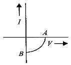
The given graph represents $V-I$ characteristic for a semiconductor device. Which of the following statements is correct?
A
It is the $V-I$ characteristic for a solar cell where point $A$ represents open circuit voltage and point $B$ represents short circuit current.
B
It is for a solar cell and points $A$ and $B$ represent open circuit voltage and current,respectively.
C
It is for a photodiode and points $A$ and $B$ represent open circuit voltage and current,respectively.
D
It is for an $LED$ and points $A$ and $B$ represent open circuit voltage and short circuit current,respectively.
Solution
(A) The $V-I$ characteristic curve shown in the graph is characteristic of a solar cell.
In this graph,the $V$-axis represents the voltage and the $I$-axis represents the current.
Point $A$ lies on the $V$-axis where the current $I = 0$,which corresponds to the open circuit voltage $(V_{OC})$.
Point $B$ lies on the $I$-axis where the voltage $V = 0$,which corresponds to the short circuit current $(I_{SC})$.
Therefore,the graph represents the $V-I$ characteristic of a solar cell where $A$ is the open circuit voltage and $B$ is the short circuit current.
0 likes
View Solution17
MediumMCQ
$A$ red $LED$ emits light at $0.1 \ W$ uniformly in all directions. The amplitude of the electric field of the light at a distance of $1 \ m$ from the diode is.... $V \ m^{-1}$
A
$2.45$
B
$5.48$
C
$7.75$
D
$9.73$
Solution
(A) The average energy density $U_{av}$ of an electromagnetic wave is given by $U_{av} = \frac{1}{2} \varepsilon_{0} E_{0}^{2}$,where $E_{0}$ is the amplitude of the electric field.
The intensity $I$ at a distance $r$ from a point source is $I = \frac{P}{4 \pi r^{2}}$.
Also,intensity is related to energy density by $I = U_{av} \times c$,where $c$ is the speed of light.
Equating the two expressions for intensity: $\frac{P}{4 \pi r^{2}} = \frac{1}{2} \varepsilon_{0} E_{0}^{2} c$.
Rearranging for $E_{0}^{2}$: $E_{0}^{2} = \frac{2P}{4 \pi r^{2} \varepsilon_{0} c} = \frac{2P}{r^{2}} \times \frac{1}{4 \pi \varepsilon_{0}} \times \frac{1}{c}$.
Given $P = 0.1 \ W$,$r = 1 \ m$,$\frac{1}{4 \pi \varepsilon_{0}} = 9 \times 10^{9} \ N \ m^{2} \ C^{-2}$,and $c = 3 \times 10^{8} \ m/s$.
$E_{0}^{2} = \frac{2 \times 0.1}{1^{2}} \times (9 \times 10^{9}) \times \frac{1}{3 \times 10^{8}} = 0.2 \times 3 \times 10 = 6$.
$E_{0} = \sqrt{6} \approx 2.45 \ V \ m^{-1}$.
0 likes
View Solution18
MediumMCQ
The $I-V$ characteristic of an $LED$ is represented by which of the following graphs?
A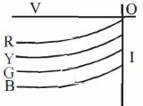
B
C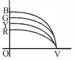
D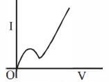
Solution
(B) An $LED$ is a forward-biased $p-n$ junction diode that emits light when current flows through it. The energy of the emitted photons is given by $E = h\nu = \frac{hc}{\lambda}$. Since $E = eV$,where $V$ is the threshold voltage,we have $eV = \frac{hc}{\lambda}$,which implies $V \propto \frac{1}{\lambda}$. Since the frequency $\nu$ is related to wavelength $\lambda$ by $\nu = \frac{c}{\lambda}$,we have $V \propto \nu$. Higher frequency light (like blue) requires a higher threshold voltage compared to lower frequency light (like red). Therefore,for a given current,the voltage required increases in the order $R < Y < G < B$. The graph that correctly depicts this forward-biased characteristic where the threshold voltage increases with frequency is the one where the curves shift to the right as we move from red to blue.
0 likes
View Solution19
MediumMCQ
Statement $-I$: $A$ photodiode operates in reverse bias.
Statement $-II$: The fractional change due to the photo-effects on the minority carrier dominated reverse bias current is more easily measurable than the fractional change in the forward bias current.
Statement $-II$: The fractional change due to the photo-effects on the minority carrier dominated reverse bias current is more easily measurable than the fractional change in the forward bias current.
A
Statement $-I$ is true,Statement $-II$ is true,Statement $-II$ is the correct explanation of Statement $-I$.
B
Statement $-I$ is true,Statement $-II$ is true,Statement $-II$ is not the correct explanation of Statement $-I$.
C
Statement $-I$ is true,Statement $-II$ is false.
D
Statement $-I$ is false,Statement $-II$ is true.
Solution
(A) photodiode is a special purpose $p-n$ junction diode fabricated with a transparent window to allow light to fall on the diode. It is operated under reverse bias.
When the photodiode is illuminated with light (photons with energy $h
u > E_g$),additional electron-hole pairs are generated.
In reverse bias,the current is primarily due to minority carriers. The fractional change in this small reverse current due to the photo-effect is significant and easily measurable.
In contrast,the forward bias current is dominated by majority carriers,which are already present in large numbers. The fractional change due to the photo-effect in forward bias is very small and difficult to detect.
Thus,both statements are true,and Statement $-II$ correctly explains why the photodiode is operated in reverse bias.
0 likes
View Solution20
MediumMCQ
Statement $-1$: $A$ photodiode operates in reverse bias.
Statement $-2$: The fractional change due to the photo-effects on the minority carrier dominated reverse bias current is more easily measurable than the fractional change in the forward bias current.
Statement $-2$: The fractional change due to the photo-effects on the minority carrier dominated reverse bias current is more easily measurable than the fractional change in the forward bias current.
A
Statement $-1$ is true,Statement $-2$ is true,Statement $-2$ is the correct explanation of Statement $-1$.
B
Statement $-1$ is true,Statement $-2$ is true,Statement $-2$ is not the correct explanation of Statement $-1$.
C
Statement $-1$ is true,Statement $-2$ is false.
D
Statement $-1$ is false,Statement $-2$ is true.
Solution
(A) photodiode is a special purpose $p-n$ junction diode fabricated with a transparent window to allow light to fall on the diode. It is operated under reverse bias conditions.
When the photodiode is illuminated with light (photons with energy $h
u > E_g$),electron-hole pairs are generated near the depletion region. Due to the electric field of the depletion region,electrons and holes are separated before they can recombine. The direction of the electric field is such that electrons reach the $n$-side and holes reach the $p$-side,giving rise to an electric current.
The reverse bias current in a $p-n$ junction is primarily due to minority charge carriers. The magnitude of this current is very small. When light falls on the junction,the number of minority carriers increases significantly,leading to a large fractional change in the reverse current. In contrast,the forward bias current is dominated by majority carriers,which are already present in large numbers. Therefore,the fractional change in forward current due to light is negligible and difficult to measure.
Thus,Statement $-1$ is true,Statement $-2$ is true,and Statement $-2$ is the correct explanation of Statement $-1$.
0 likes
View Solution21
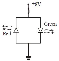
DifficultMCQ
The figure shows $2$ $LEDs$ that can be used as a polarity detector. Applying a positive source voltage results in a green light,while negative supplies result in a red light. Packages of such combinations are commercially available. Find the resistor $R$ to ensure a current of $20 \ mA$ through the $ON$ diode for the configuration. Both diodes have a reverse breakdown voltage of $3 \ V$ and an average turn-on voltage of $2 \ V$. The source voltage is $8 \ V$. Find $R$ in $\Omega$.
A
$250$
B
$300$
C
$325$
D
$400$
Solution
(B) When a positive voltage of $8 \ V$ is applied,the green $LED$ is forward-biased and conducts,while the red $LED$ is reverse-biased.
The current $I$ flowing through the circuit is given by Ohm's law:
$I = \frac{V_{source} - V_{LED}}{R}$
Given $I = 20 \ mA = 20 \times 10^{-3} \ A$,$V_{source} = 8 \ V$,and $V_{LED} = 2 \ V$:
$20 \times 10^{-3} = \frac{8 - 2}{R}$
$R = \frac{6 \ V}{20 \times 10^{-3} \ A} = \frac{6000}{20} \ \Omega = 300 \ \Omega$
The reverse voltage across the red $LED$ is $2 \ V$,which is less than its reverse breakdown voltage of $3 \ V$,so it is safe.
0 likes
View Solution22
MediumMCQ
For $LED$s to emit light in the visible region of the electromagnetic spectrum,they should have an energy band gap in the range of:
A
$0.1 \, eV$ to $0.4 \, eV$
B
$0.5 \, eV$ to $0.8 \, eV$
C
$0.9 \, eV$ to $1.6 \, eV$
D
$1.7 \, eV$ to $3.0 \, eV$
Solution
(D) The energy of a photon emitted by an $LED$ is approximately equal to the energy band gap $E_g$ of the semiconductor material.
The relationship between energy and wavelength is given by $E_g = \frac{hc}{\lambda}$.
The visible region of the electromagnetic spectrum corresponds to wavelengths ranging from approximately $400 \, nm$ to $700 \, nm$ (i.e.,$4 \times 10^{-7} \, m$ to $7 \times 10^{-7} \, m$).
For $\lambda = 700 \, nm$ $(7 \times 10^{-7} \, m)$:
$E_g = \frac{6.63 \times 10^{-34} \times 3 \times 10^8}{7 \times 10^{-7}} \approx 2.84 \times 10^{-19} \, J \approx 1.77 \, eV$.
For $\lambda = 400 \, nm$ $(4 \times 10^{-7} \, m)$:
$E_g = \frac{6.63 \times 10^{-34} \times 3 \times 10^8}{4 \times 10^{-7}} \approx 4.97 \times 10^{-19} \, J \approx 3.1 \, eV$.
Thus,for an $LED$ to emit light in the visible region,the energy band gap should be in the range of approximately $1.7 \, eV$ to $3.0 \, eV$.
0 likes
View Solution23
EasyMCQ
$A$ photo cell is a device used to:
A
Store photons
B
Measure light intensity
C
Convert photon energy into mechanical energy
D
Store electrical energy for replacing storage batteries
Solution
(B) photo cell (or photodiode) operates on the principle of the photoelectric effect. When light falls on the photosensitive surface,it emits electrons. The number of photoelectrons emitted is directly proportional to the intensity of the incident light. By measuring the photocurrent,we can determine the intensity of the light. Therefore,a photo cell is used to measure light intensity.
0 likes
View Solution24
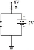
MediumMCQ
$A$ light emitting diode $(LED)$ has a voltage drop of $2\,V$ across it and passes a current of $10\,mA$ when it operates with a $6\,V$ battery through a limiting resistor $R$. The value of $R$ is $......\,k\Omega$.
A
$0.4$
B
$0.6$
C
$0.2$
D
$400$
Solution
(A) The $LED$ is connected in series with a resistor $R$ and a $6\,V$ battery.
Since the $LED$ and the resistor are in series,the current flowing through both is the same,$I = 10\,mA = 10 \times 10^{-3}\,A$.
The voltage drop across the $LED$ is $V_{LED} = 2\,V$.
The total voltage of the battery is $V = 6\,V$.
According to Kirchhoff's voltage law,the voltage drop across the resistor $R$ is $V_R = V - V_{LED} = 6\,V - 2\,V = 4\,V$.
Using Ohm's law,$V_R = I \times R$,we get $R = \frac{V_R}{I}$.
Substituting the values: $R = \frac{4\,V}{10 \times 10^{-3}\,A} = 0.4 \times 10^3\,\Omega = 400\,\Omega$.
Since $1\,k\Omega = 1000\,\Omega$,then $400\,\Omega = 0.4\,k\Omega$.
0 likes
View Solution25
MediumMCQ
To measure light intensity,we use:
A
$LED$ with forward bias
B
$LED$ with reverse bias
C
photodiode with reverse bias
D
photodiode with forward bias
Solution
(C) For detecting the intensity of light,we use a photodiode in reverse bias.
When a photodiode is reverse-biased,the width of the depletion layer increases compared to forward bias,and a small reverse current (dark current) flows through the diode.
When light is incident on the junction,electron-hole pairs are generated in the depletion layer in large amounts due to the broad depletion layer. These charge carriers can easily cross the barrier,contributing to the current across the diode.
Therefore,in reverse bias,the diode converts incident light into current more significantly due to the broad depletion layer,making the photocurrent significant compared to the forward bias current.
0 likes
View Solution26
DifficultMCQ
$A$ Light Emitting Diode $(LED)$ has a voltage drop of $2\,V$ across it and passes a current of $10\,mA$ when it operates with a $6\,V$ battery through a limiting resistor $R$. The value of $R$ is.........$k\,\Omega$.
A
$0.4$
B
$4$
C
$40$
D
$400$
Solution
(A) Light Emitting Diode $(LED)$ is a forward-biased $P-N$ junction that emits light.
The voltage drop across the $LED$ is $V_{LED} = 2\,V$.
The battery voltage is $V_{battery} = 6\,V$.
The voltage across the limiting resistor $R$ is $V_R = V_{battery} - V_{LED} = 6\,V - 2\,V = 4\,V$.
The current flowing through the circuit is $I = 10\,mA = 10 \times 10^{-3}\,A = 0.01\,A$.
Using Ohm's law,$V_R = I \times R$,we get $R = V_R / I$.
$R = 4\,V / 0.01\,A = 400\,\Omega$.
Since $1\,k\Omega = 1000\,\Omega$,we have $R = 400 / 1000 = 0.4\,k\Omega$.
0 likes
View Solution27
EasyMCQ
Select the correct statement.
A
Photodiode works in forward biasing.
B
$LED$ works in reverse biasing.
C
In solar cell,$GaAs$ is preferred over $Si$.
D
Doping of Zener diode is small.
Solution
(C) $1$. $A$ photodiode is operated in reverse bias to detect optical signals. Thus,option $A$ is incorrect.
$2$. An $LED$ (Light Emitting Diode) works in forward bias to emit light. Thus,option $B$ is incorrect.
$3$. $GaAs$ (Gallium Arsenide) has a band gap of approximately $1.5 \ eV$,which is ideal for solar energy conversion compared to $Si$ $(1.1 \ eV)$. It also has a higher absorption coefficient. Thus,option $C$ is correct.
$4$. $A$ Zener diode is heavily doped to allow for a sharp breakdown voltage. Thus,option $D$ is incorrect.
0 likes
View Solution28
DifficultMCQ
The photodiode is made of a material with a band gap of $2.0\, eV$. The minimum frequency of the radiation that can be absorbed by the material is nearly
A
$1\times10^{14}\, Hz$
B
$20\times10^{14}\, Hz$
C
$10\times10^{14}\, Hz$
D
$5\times10^{14}\, Hz$
Solution
(D) The energy of a photon required to excite an electron across the band gap is given by $E = h\nu$,where $E$ is the band gap energy,$h$ is Planck's constant,and $\nu$ is the frequency.
Given,$E = 2.0\, eV = 2.0 \times 1.6 \times 10^{-19}\, J = 3.2 \times 10^{-19}\, J$.
Planck's constant $h \approx 6.63 \times 10^{-34}\, J\cdot s$.
The minimum frequency $\nu$ is given by $\nu = E / h$.
$\nu = (3.2 \times 10^{-19}) / (6.63 \times 10^{-34}) \approx 0.4826 \times 10^{15}\, Hz$.
$\nu \approx 4.83 \times 10^{14}\, Hz$.
Rounding to the nearest option,we get $\nu \approx 5 \times 10^{14}\, Hz$.
0 likes
View Solution29
EasyMCQ
Which wavelength of the Sun is primarily used to generate electric energy in solar cells?
A
Radio waves
B
Infrared waves
C
Visible light
D
Microwaves
Solution
(B) Solar cells are semiconductor devices that convert light energy directly into electrical energy via the photovoltaic effect. While solar radiation covers a broad spectrum,the efficiency of silicon-based solar cells is highest for the visible and near-infrared regions of the solar spectrum. Infrared waves,in particular,contribute significantly to the thermal and energy conversion processes in solar technologies. Therefore,option $(b)$ is the most appropriate choice among the given options.
0 likes
View Solution30
MediumMCQ
An $LED$ (Light Emitting Diode) is constructed from a $p-n$ junction based on a certain $Ga-As-P$ semiconducting material whose energy gap is $1.9\, eV$. What is the wavelength of the emitted light?
A
$650\, nm$
B
$65\, \mathring{A}$
C
$800\, nm$
D
$8000\, \mathring{A}$
Solution
(A) The wavelength $\lambda$ of the emitted light is given by the relation:
$\lambda = \frac{hc}{E_g}$
where $h = 6.63 \times 10^{-34} \, J \cdot s$ is Planck's constant,$c = 3 \times 10^8 \, m/s$ is the speed of light,and $E_g$ is the energy gap.
Given $E_g = 1.9 \, eV = 1.9 \times 1.6 \times 10^{-19} \, J$.
Substituting the values:
$\lambda = \frac{6.63 \times 10^{-34} \times 3 \times 10^8}{1.9 \times 1.6 \times 10^{-19}} \, m$
$\lambda \approx \frac{19.89 \times 10^{-26}}{3.04 \times 10^{-19}} \, m$
$\lambda \approx 6.54 \times 10^{-7} \, m$
$\lambda \approx 654 \times 10^{-9} \, m = 654 \, nm$.
Rounding to the nearest provided option,the wavelength is $650 \, nm$.
0 likes
View Solution31
EasyMCQ
Assertion: $A$ $p-n$ junction with reverse bias can be used as a photo-diode to measure light intensity.
Reason: In a reverse bias condition,the current is small but is more sensitive to changes in incident light intensity.
Reason: In a reverse bias condition,the current is small but is more sensitive to changes in incident light intensity.
A
If both Assertion and Reason are correct and the Reason is a correct explanation of the Assertion.
B
If both Assertion and Reason are correct but Reason is not a correct explanation of the Assertion.
C
If the Assertion is correct but Reason is incorrect.
D
If both the Assertion and Reason are incorrect.
Solution
(A) photo-diode is a reverse-biased $p-n$ junction diode. At the $p-n$ junction,there exists a junction electric field which,at equilibrium,does not permit the flow of charge carriers across the junction.
When such a $p-n$ diode is illuminated with light photons having energy $h
u > E_{g}$,electron-hole pairs are generated in the depletion layer (or near the junction). These charge carriers are separated by the junction field and made to flow across the junction,resulting in a change in the reverse saturation current.
Because the reverse current is highly sensitive to the generation of these photo-excited carriers,the change in current is directly proportional to the incident light intensity. Thus,the device acts as a photo-detector.
0 likes
View Solution32
EasyMCQ
Assertion : Diode lasers are used as optical sources in optical communication.
Reason : Diode lasers consume less energy.
Reason : Diode lasers consume less energy.
A
If both Assertion and Reason are correct and the Reason is a correct explanation of the Assertion.
B
If both Assertion and Reason are correct but Reason is not a correct explanation of the Assertion.
C
If the Assertion is correct but Reason is incorrect.
D
If both the Assertion and Reason are incorrect.
Solution
(A) Diode lasers are widely used in optical communication because they are compact,have high efficiency,and can be easily modulated at high frequencies.
They also consume significantly less energy compared to other light sources like gas lasers or incandescent bulbs.
Since the high efficiency and low energy consumption are key reasons for their preference in optical communication,the Reason correctly explains the Assertion.
They also consume significantly less energy compared to other light sources like gas lasers or incandescent bulbs.
Since the high efficiency and low energy consumption are key reasons for their preference in optical communication,the Reason correctly explains the Assertion.
0 likes
View Solution33
EasyMCQ
An $LED$ is constructed from a $p-n$ junction diode using $GaAsP$. The energy gap is $1.9\; eV$. The wavelength of the light emitted will be equal to
A
$10.4 \times 10^{-26}\; m$
B
$654 \;nm$
C
$654 \;\mathring A$
D
$654 \times 10^{-11} \;m$
Solution
(B) The energy of the emitted photon is given by $E = \frac{hc}{\lambda}$.
Given the energy gap $E_g = 1.9\; eV$.
The wavelength $\lambda$ is calculated using the formula $\lambda = \frac{hc}{E_g}$.
Using the approximation $hc \approx 1240\; eV \cdot nm$,we get:
$\lambda = \frac{1240\; eV \cdot nm}{1.9\; eV} \approx 652.6\; nm$.
Rounding to the nearest provided option,we get $\lambda \approx 654\; nm$.
0 likes
View Solution34
Medium
$A$ family uses $8 \; kW$ of power.
$(a)$ Direct solar energy is incident on the horizontal surface at an average rate of $200 \; W$ per square meter. If $20 \%$ of this energy can be converted to useful electrical energy, how large an area is needed to supply $8 \; kW$?
$(b)$ Compare this area to that of the roof of a typical house.
$(a)$ Direct solar energy is incident on the horizontal surface at an average rate of $200 \; W$ per square meter. If $20 \%$ of this energy can be converted to useful electrical energy, how large an area is needed to supply $8 \; kW$?
$(b)$ Compare this area to that of the roof of a typical house.
Solution
(N/A) Power used by the family, $P = 8 \; kW = 8 \times 10^{3} \; W$.
Solar energy received per square meter $= 200 \; W/m^{2}$.
Efficiency of conversion from solar to electrical energy $= 20 \% = 0.2$.
Let the area required to generate the desired electricity be $A$.
The useful power generated is given by: $P = \text{Efficiency} \times \text{Area} \times \text{Incident solar energy rate}$.
$8 \times 10^{3} = 0.2 \times A \times 200$.
$8000 = 40 \times A$.
$A = \frac{8000}{40} = 200 \; m^{2}$.
$(b)$ The area of a solar panel required to generate $8 \; kW$ of electricity is $200 \; m^{2}$. $A$ typical house roof has dimensions roughly $14 \; m \times 14 \; m = 196 \; m^{2}$. Thus, the required area is approximately equivalent to the roof area of a typical house.
0 likes
View Solution35
Medium
The current in the forward bias is known to be more $(\sim mA)$ than the current in the reverse bias $(\sim \mu A)$. What is the reason then to operate the photodiodes in reverse bias?
Solution
(N/A) Consider the case of an $n$-type semiconductor. Obviously,the majority carrier density $(n)$ is considerably larger than the minority hole density $(p)$ (i.e.,$n \gg p$). On illumination,let the excess electrons and holes generated be $\Delta n$ and $\Delta p$,respectively:
$n^{\prime} = n + \Delta n$
$p^{\prime} = p + \Delta p$
Here,$n^{\prime}$ and $p^{\prime}$ are the electron and hole concentrations at any particular illumination,and $n$ and $p$ are carrier concentrations when there is no illumination. Remember $\Delta n = \Delta p$ and $n \gg p$.
Hence,the fractional change in the majority carriers (i.e.,$\Delta n / n$) would be much less than that in the minority carriers (i.e.,$\Delta p / p$). In general,we can state that the fractional change due to the photo-effects on the minority carrier-dominated reverse bias current is more easily measurable than the fractional change in the forward bias current. Hence,photodiodes are preferably used in the reverse bias condition for measuring light intensity.
0 likes
View Solution36
Medium
Why are $Si$ and $GaAs$ preferred materials for solar cells?
Solution
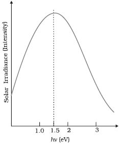
(N/A) The solar radiation spectrum received by us is shown in the figure.
The maxima is near $1.5 \, eV$. For photo-excitation,$h\nu > E_g$. Hence,a semiconductor with a band gap $\sim 1.5 \, eV$ or lower is likely to give better solar conversion efficiency. Silicon has $E_g \sim 1.1 \, eV$ while for $GaAs$ it is $1.53 \, eV$.
In fact,$GaAs$ is better (in spite of its higher band gap) than $Si$ because of its relatively higher absorption coefficient. If we choose materials like $CdS$ or $CdSe$ $(E_g \sim 2.4 \, eV)$,we can use only the high-energy component of the solar energy for photo-conversion,and a significant part of the energy will be of no use.
The question arises: why do we not use a material like $PbS$ $(E_g \sim 0.4 \, eV)$ which satisfies the condition $h\nu > E_g$ for $\nu$ maxima corresponding to the solar radiation spectra? If we do so,most of the solar radiation will be absorbed on the top layer of the solar cell and will not reach in or near the depletion region. For effective electron-hole separation,due to the junction field,we want the photo-generation to occur in the junction region only.
0 likes
View Solution37
Medium
$A$ $p-n$ photodiode is fabricated from a semiconductor with a band gap of $2.8 \; eV$. Can it detect a wavelength of $6000 \; nm$?
Solution
(NO) The energy band gap of the given photodiode is $E_g = 2.8 \; eV$.
The wavelength of the incident light is $\lambda = 6000 \; nm = 6000 \times 10^{-9} \; m$.
The energy of a photon is given by the relation $E = \frac{hc}{\lambda}$.
Using $h = 6.626 \times 10^{-34} \; Js$ and $c = 3 \times 10^8 \; m/s$:
$E = \frac{6.626 \times 10^{-34} \times 3 \times 10^8}{6000 \times 10^{-9}} \; J = 3.313 \times 10^{-20} \; J$.
Converting this energy into electron-volts $(eV)$:
$E = \frac{3.313 \times 10^{-20}}{1.6 \times 10^{-19}} \; eV \approx 0.207 \; eV$.
Since the energy of the incident photon $(0.207 \; eV)$ is less than the band gap energy of the photodiode $(2.8 \; eV)$,the photodiode cannot detect the signal of wavelength $6000 \; nm$.
0 likes
View Solution38
Difficult
What are optoelectronic devices? Give the names of such major devices.
Solution
(N/A) Optoelectronic devices are semiconductor devices that convert light energy into electrical energy or vice versa,based on the interaction of light with semiconductor materials.
The major optoelectronic devices are as follows:
$(1)$ Photodiodes: These are used for detecting optical signals (photodetectors).
$(2)$ Light Emitting Diodes $(LED)$: These devices convert electrical energy into light energy.
$(3)$ Photovoltaic devices: These convert optical radiation into electricity (e.g.,solar cells).
0 likes
View Solution39
Medium
Explain the construction and working of a photodiode.
Solution
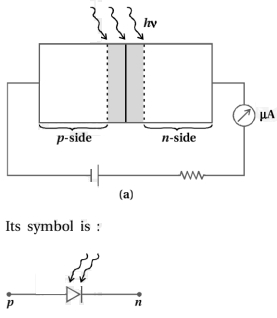
(N/A) photodiode is a special-purpose $p-n$ junction diode.
It is fabricated with a transparent window to allow light to fall on the diode.
When the photodiode is illuminated with light (photons) having energy $(h\nu)$ greater than the energy gap $(E_g)$ of the semiconductor,electron-hole $(e-h)$ pairs are generated due to the absorption of photons.
The illuminated photodiode in reverse bias is shown in the figure.
The diode is fabricated such that the generation of $(e-h)$ pairs takes place in or near the depletion region of the diode.
Due to the electric field of the junction,electrons and holes are separated before they can recombine.
The direction of the electric field is such that electrons reach the $n$-side and holes reach the $p$-side.
Electrons are collected on the $n$-side and holes are collected on the $p$-side,giving rise to an electromotive force $(emf)$. When an external load is connected,current flows through the circuit.
The magnitude of the photocurrent depends on the intensity of the incident light; the photocurrent is proportional to the incident light intensity.
When a reverse bias is applied,the current changes significantly with changes in light intensity.
0 likes
View Solution40
Medium
Explain the design,working,uses,and benefits of a light-emitting diode $(LED)$.
Solution
(N/A) Design: An $LED$ is a heavily doped $p-n$ junction diode. It is encapsulated in a transparent cover so that the emitted light can escape. It is operated under forward bias.
Working: When the diode is forward-biased,electrons are injected from the $n$-region to the $p$-region,and holes are injected from the $p$-region to the $n$-region. Near the junction boundary,the concentration of these minority carriers increases. These excess minority carriers recombine with majority carriers near the junction. During this recombination,energy is released in the form of photons. The energy of the emitted photons is approximately equal to or slightly less than the band gap energy $(E_g)$. As forward current increases,the intensity of light increases,reaches a maximum,and then decreases due to heating effects.
Uses: $LED$s are used in remote controls,optical communication,traffic signals,decorative lighting,and displays.
Benefits: $LED$s have low operational voltage,fast action,no warm-up time required,long life,ruggedness,and they are available in different colors.
0 likes
View Solution41
Medium
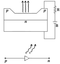
Describe the construction, working, and use of a solar cell.
Solution
(N/A) solar cell is essentially a $p-n$ junction that generates an electromotive force $(emf)$ when solar radiation falls on the junction. Sunlight is not strictly required; any light with photon energy greater than the band gap energy $(E_{g})$ of the semiconductor can produce a photovoltage. The working principle of a solar cell is based on the photovoltaic effect, similar to a photodiode, but it does not require an external bias voltage.
Construction:
$1$. $A$ $p-Si$ wafer of about $300 \mu m$ thickness is taken.
$2$. $A$ thin layer $(\, 0.3 \mu m)$ of $n-Si$ is grown on one side by a diffusion process to form a $p-n$ junction.
$3$. The bottom of the $p-Si$ wafer is coated with a metal to form the back contact.
$4$. On the top of the $n-Si$ layer, a metallic grid (or finger electrode) is deposited to serve as the front contact. This grid covers only a small fraction of the area $( < 15 \%)$ to allow maximum light incidence.
Working:
The generation of $emf$ occurs through three basic processes:
$(1)$ Generation of electron-hole $(e-h)$ pairs due to light absorption $(h\nu > E_{g})$ near the junction.
$(2)$ Separation of electrons and holes due to the electric field of the depletion region. Electrons are swept to the $n$-side and holes to the $p$-side.
$(3)$ Collection of charges: Electrons reaching the $n$-side are collected by the front contact, and holes reaching the $p$-side are collected by the back contact. This makes the $p$-side positive and the $n$-side negative, creating a photovoltage.
Use:
Solar cells are used in calculators, watches, satellites, and for power generation in remote areas.
0 likes
View Solution42
Easy
What are the ideal materials for the fabrication of a solar cell? Give the criteria for their selection.
Solution
(N/A) Semiconductors with a band gap close to $1.5 \text{ eV}$ are ideal materials for solar cell fabrication.
These materials include:
$Si$ $(E_{g} = 1.1 \text{ eV})$,
$GaAs$ $(E_{g} = 1.43 \text{ eV})$,
$CdTe$ $(E_{g} = 1.45 \text{ eV})$,
$CuInSe_{2}$ $(E_{g} = 1.04 \text{ eV})$,etc.
The following are the important criteria for selecting the right materials for fabricating a solar cell:
$(1)$ Band gap $E_{g}$ should be in the range of $1.0 \text{ eV}$ to $1.8 \text{ eV}$.
$(2)$ High optical absorption,approximately $10^{4} \text{ cm}^{-1}$.
$(3)$ High electrical conductivity.
$(4)$ The raw material should be easily available.
$(5)$ The cost of the material should be low.
0 likes
View Solution43
EasyMCQ
What type of $p-n$ junction diode does not require forward bias to operate?
A
Light Emitting Diode $(LED)$
B
Zener Diode
C
Photodiode
D
Solar Cell
Solution
(D) $p-n$ junction diode that does not require forward bias to operate is a $Solar$ $Cell$.
$A$ $Solar$ $Cell$ is a photovoltaic device that converts solar energy directly into electrical energy.
Unlike an $LED$ or a standard diode,which require an external voltage source (forward bias) to function,a $Solar$ $Cell$ generates an electromotive force $(EMF)$ when light photons with energy greater than the bandgap energy of the semiconductor material fall on the junction.
This process is known as the photovoltaic effect.
0 likes
View Solution44
EasyMCQ
What kind of $p-n$ junction diode does not require any kind of bias?
A
Light Emitting Diode ($L$.$E$.$D$)
B
Photodiode
C
Solar Cell
D
Zener Diode
Solution
(C) $p-n$ junction diode that does not require any external bias to function is a $Solar \ Cell$.
In a $Solar \ Cell$,the generation of electromotive force $(EMF)$ occurs due to the absorption of light (photons) by the semiconductor material.
When light with energy greater than the bandgap energy $(E_g)$ falls on the $p-n$ junction,electron-hole pairs are generated.
These charge carriers are separated by the junction's electric field,creating a potential difference across the device without the need for an external voltage source.
0 likes
View Solution45
EasyMCQ
What kind of diode is used as a photo detector?
A
Light Emitting Diode ($L$.$E$.$D$)
B
Photodiode
C
Zener Diode
D
Junction Diode
Solution
(B) photodiode is a special type of $p-n$ junction diode that is designed to operate under reverse bias conditions.
When light (photons) with energy greater than the bandgap energy of the semiconductor falls on the junction,it generates electron-hole pairs.
These charge carriers are swept across the junction by the electric field in the depletion region,creating a photocurrent.
Because of this property,it is used as a light detector to convert optical signals into electrical signals.
0 likes
View Solution46
Easy
State the band gap of the semiconductor used in the making of $LED$.
Solution
(N/A) The band gap of the semiconductor used in the making of a Light Emitting Diode $(LED)$ is typically in the range of $1.8 \ eV$ to $3.0 \ eV$.
This energy range corresponds to the visible spectrum of light,allowing the $LED$ to emit light in colors ranging from red to violet.
The specific band gap depends on the material composition of the semiconductor used (e.g.,Gallium Arsenide Phosphide or Gallium Nitride).
This energy range corresponds to the visible spectrum of light,allowing the $LED$ to emit light in colors ranging from red to violet.
The specific band gap depends on the material composition of the semiconductor used (e.g.,Gallium Arsenide Phosphide or Gallium Nitride).
0 likes
View Solution47
Medium
Why is the $I-V$ characteristic of a solar cell drawn in the fourth quadrant of the coordinate system?
Solution
(N/A) solar cell is a device that converts light energy into electrical energy. It acts as a source of power rather than a consumer of power.
In the $I-V$ characteristic graph,the $V$-axis represents the voltage across the device,and the $I$-axis represents the current flowing through it.
For a solar cell,the generated current $(I)$ flows out of the device,which is considered negative by convention in the circuit,while the voltage $(V)$ across the terminals is positive.
Since the current is negative $(I < 0)$ and the voltage is positive $(V > 0)$,the operating point lies in the fourth quadrant of the Cartesian coordinate system.
This indicates that the solar cell is delivering power to an external load.
0 likes
View Solution48
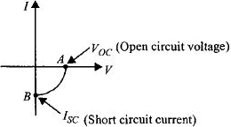
Medium
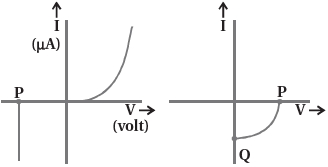
$(i)$ Name the type of diode whose characteristics are shown in figure $(a)$ and figure $(b)$.
$(ii)$ What does the point $P$ in figure $(a)$ represent?
$(iii)$ What do the points $P$ and $Q$ in figure $(b)$ represent?
$(ii)$ What does the point $P$ in figure $(a)$ represent?
$(iii)$ What do the points $P$ and $Q$ in figure $(b)$ represent?
Solution
(N/A) $(i)$ Figure $(a)$ shows the characteristics of a Zener diode,and figure $(b)$ shows the characteristics of a solar cell.
$(ii)$ Point $P$ in figure $(a)$ represents the reverse breakdown voltage,also known as the Zener voltage $(V_Z)$.
$(iii)$ Point $P$ in figure $(b)$ represents the open-circuit voltage $(V_{OC})$. This is the voltage across the solar cell when the net current through it is zero. At this point,the forward current due to the applied voltage exactly cancels the photocurrent generated by light.
Point $Q$ in figure $(b)$ represents the short-circuit current $(I_{SC})$. This is the current flowing through the solar cell when the external voltage applied across it is zero,under illumination.
0 likes
View Solution49
EasyMCQ
Three photodiodes $D_1, D_2,$ and $D_3$ are made of semiconductors having band gaps of $2.5 \ eV, 2 \ eV,$ and $3 \ eV,$ respectively. Which ones will be able to detect light of wavelength $6000 \ \mathring{A}$?
A
$D_1$ only
B
$D_1$ and $D_2$
C
$D_2$ and $D_3$
D
$D_1$ and $D_3$
Solution
(B) photodiode can detect light if the energy of the incident photon $(E)$ is greater than the band gap energy $(E_g)$ of the semiconductor material.
The energy of a photon with wavelength $\lambda = 6000 \ \mathring{A}$ is given by:
$E = \frac{hc}{\lambda} = \frac{12400 \ eV \cdot \mathring{A}}{6000 \ \mathring{A}} \approx 2.07 \ eV$.
For detection,we require $E > E_g$:
$1$. For $D_1$: $E_g = 2.5 \ eV$. Since $2.07 \ eV < 2.5 \ eV$,$D_1$ cannot detect this light.
$2$. For $D_2$: $E_g = 2.0 \ eV$. Since $2.07 \ eV > 2.0 \ eV$,$D_2$ can detect this light.
$3$. For $D_3$: $E_g = 3.0 \ eV$. Since $2.07 \ eV < 3.0 \ eV$,$D_3$ cannot detect this light.
Therefore,only $D_2$ will be able to detect the light. However,based on the provided options,if the question implies detection for $E \ge E_g$,only $D_2$ works. Given the standard options for this problem,$D_1$ and $D_2$ are often cited if the wavelength is slightly different,but here $D_2$ is the only one strictly satisfying the condition.
0 likes
View SolutionSemiconductor Electronics — Light Emitting Diode (L.E.D), Photodiode, Solar Cell · Frequently Asked Questions
1Are these Semiconductor Electronics questions useful for JEE and NEET?
Yes. All questions in this section are mapped to JEE Main and NEET exam patterns. Previous year questions from JEE Main, NEET, GUJCET and state-level exams are included with full solutions.
2Can I switch to Hindi or Gujarati for these questions?
Yes. Use the language tabs in the hero section or the sidebar to view the same questions and solutions in English, Hindi or Gujarati.
3How do I generate a question paper from this subtopic?
Use the Vedclass Exam Paper Generator — select the chapter and subtopic, set difficulty, and generate Sets A, B, C, D automatically. First 3 chapters of every subject are free.
Vedclass Products
For Students
Vedclass Test Series
Mock tests in real JEE/NEET style with performance analysis. 5-day free trial.
Start Free TrialFor Teachers
Exam Paper Generator
Generate Set A/B/C/D papers from this chapter in 2 minutes. 3 chapters free.
Try FreeFor Institutes
Online Exam Module
Live online exams with unlimited students, 360° analytics & white-label branding.
See DemoFor Teachers & Institutes
Generate a Semiconductor Electronics Exam Paper in 2 Minutes
Select subtopic & difficulty — Sets A, B, C, D auto-generated with No Repeat logic.
First 3 chapters of every subject are free — no payment required.