
A English
Classification of Materials and Energy Band Theory Questions in English
Class 12 Physics · Semiconductor Electronics · Classification of Materials and Energy Band Theory
190+
Questions
English
Language
100%
With Solutions
Showing 48 of 190 questions in English
1
EasyMCQ
$\sigma_1$ and $\sigma_2$ are the electrical conductivities of $Ge$ and $Na$ respectively. If these substances are heated,then
A
Both $\sigma_1$ and $\sigma_2$ increase
B
$\sigma_1$ increases and $\sigma_2$ decreases
C
$\sigma_1$ decreases and $\sigma_2$ increases
D
Both $\sigma_1$ and $\sigma_2$ decrease
Solution
(B) $Ge$ (Germanium) is a semiconductor,and $Na$ (Sodium) is a metal.
For semiconductors,the number of charge carriers increases significantly with an increase in temperature,leading to an increase in electrical conductivity ($\sigma_1$ increases).
For metals,the increase in temperature leads to increased lattice vibrations (collisions),which increases the resistivity and consequently decreases the electrical conductivity ($\sigma_2$ decreases).
Therefore,$\sigma_1$ increases and $\sigma_2$ decreases.
0 likes
View Solution2
EasyMCQ
For a crystal system where $a = b = c$ and $\alpha = \beta = \gamma \neq 90^\circ$,the system is:
A
Tetragonal system
B
Cubic system
C
Orthorhombic system
D
Rhombohedral system
Solution
(D) The crystal system defined by the parameters $a = b = c$ and $\alpha = \beta = \gamma \neq 90^\circ$ is known as the Rhombohedral (or Trigonal) system.
$1$. For a Cubic system: $a = b = c$ and $\alpha = \beta = \gamma = 90^\circ$.
$2$. For a Tetragonal system: $a = b \neq c$ and $\alpha = \beta = \gamma = 90^\circ$.
$3$. For an Orthorhombic system: $a \neq b \neq c$ and $\alpha = \beta = \gamma = 90^\circ$.
$4$. For a Rhombohedral system: $a = b = c$ and $\alpha = \beta = \gamma \neq 90^\circ$.
Therefore,the correct option is $D$.
0 likes
View Solution3
EasyMCQ
The expected energy of the electrons at absolute zero is called
A
Fermi energy
B
Emission energy
C
Work function
D
Potential energy
Solution
(A) The highest energy level that an electron can occupy in a material at absolute zero temperature $(0 \ K)$ is known as the Fermi energy level. Therefore,the correct answer is Fermi energy.
0 likes
View Solution4
EasyMCQ
Metallic solids are always opaque because
A
Solids affect the incident light
B
Incident light is readily absorbed by the free electrons in a metal
C
Incident light is scattered by solid molecules
D
Energy band traps the incident light
Solution
(B) Metallic solids are opaque because the incident light is readily absorbed by the free electrons present in the metal.
These free electrons oscillate in response to the oscillating electric field of the incident light,absorbing the energy and preventing the light from passing through the material.
These free electrons oscillate in response to the oscillating electric field of the incident light,absorbing the energy and preventing the light from passing through the material.
0 likes
View Solution5
EasyMCQ
In which of the following is an ionic bond present?
A
$NaCl$
B
$Ar$
C
$Si$
D
$Ge$
Solution
(A) In ionic bonding,electrons are transferred from one type of atom to another,creating positive and negative ions.
For example,in $NaCl$,the $Na$ atom loses one electron and the $Cl$ atom gains one electron.
This results in the formation of $Na^{+}$ and $Cl^{-}$ ions,which achieve a stable noble gas shell structure.
For example,in $NaCl$,the $Na$ atom loses one electron and the $Cl$ atom gains one electron.
This results in the formation of $Na^{+}$ and $Cl^{-}$ ions,which achieve a stable noble gas shell structure.
0 likes
View Solution6
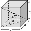
DifficultMCQ
The distance between the body-centered atom and a corner atom in sodium $(a = 4.225 \, \mathring{A})$ is ....... $\mathring{A}$ $[AIPMT \, 1995]$
A
$3.66$
B
$3.17$
C
$2.99$
D
$2.54$
Solution
(A) Sodium crystallizes in a body-centered cubic $(BCC)$ structure.
In a $BCC$ unit cell,the body-centered atom lies at the center of the body diagonal.
The length of the body diagonal is $\sqrt{3}a$,where $a$ is the edge length of the cube.
The distance between the body-centered atom and a corner atom is half of the body diagonal.
Distance $= \frac{\sqrt{3}a}{2}$
Given $a = 4.225 \, \mathring{A}$.
Distance $= \frac{\sqrt{3} \times 4.225}{2} \approx \frac{1.732 \times 4.225}{2} \approx \frac{7.3177}{2} \approx 3.6588 \, \mathring{A} \approx 3.66 \, \mathring{A}$.
0 likes
View Solution7
MediumMCQ
Sodium has a body-centered cubic $(BCC)$ packing. If the distance between two nearest atoms is $3.7 \mathring{A}$,then its lattice parameter is.....$\mathring{A}$
A
$4.8$
B
$4.3$
C
$3.9$
D
$3.3$
Solution
(B) For a body-centered cubic $(BCC)$ structure,the nearest neighbor distance $d$ is given by the distance between the corner atom and the body-centered atom.
In a $BCC$ unit cell with lattice parameter $a$,the body diagonal is $\sqrt{3}a$.
The distance between the nearest atoms is $d = \frac{\sqrt{3}a}{2}$.
Given $d = 3.7 \mathring{A}$,we can solve for $a$:
$a = \frac{2d}{\sqrt{3}} = \frac{2 \times 3.7}{1.732} \approx 4.27 \mathring{A}$.
Rounding to one decimal place,we get $a = 4.3 \mathring{A}$.
0 likes
View Solution8
EasyMCQ
In good conductors of electricity,the type of bonding that exists is
A
Ionic
B
Vander Waals
C
Covalent
D
Metallic
Solution
(D) In good conductors of electricity,such as metals,the atoms are held together by metallic bonding.
In this type of bonding,the valence electrons are not bound to any specific atom but are free to move throughout the crystal lattice,forming a 'sea of electrons'.
This mobility of electrons is the fundamental reason why metals are excellent conductors of electricity.
In this type of bonding,the valence electrons are not bound to any specific atom but are free to move throughout the crystal lattice,forming a 'sea of electrons'.
This mobility of electrons is the fundamental reason why metals are excellent conductors of electricity.
0 likes
View Solution9
EasyMCQ
Bonding in a germanium crystal (semiconductor) is:
A
Metallic
B
Ionic
C
Van der Waals type
D
Covalent
Solution
(D) Germanium $(Ge)$ is a Group-$14$ element in the periodic table.
In a germanium crystal,each germanium atom shares its four valence electrons with four neighboring germanium atoms to complete its octet.
This sharing of electrons results in the formation of covalent bonds.
Therefore,the bonding in a germanium crystal is covalent.
In a germanium crystal,each germanium atom shares its four valence electrons with four neighboring germanium atoms to complete its octet.
This sharing of electrons results in the formation of covalent bonds.
Therefore,the bonding in a germanium crystal is covalent.
0 likes
View Solution10
EasyMCQ
When the electrical conductivity of a semiconductor is due to the breaking of its covalent bonds,then the semiconductor is said to be
A
Donor
B
Acceptor
C
Intrinsic
D
Extrinsic
Solution
(C) An intrinsic semiconductor is a pure semiconductor material in which the electrical conductivity is solely due to the thermal excitation of electrons from the valence band to the conduction band,which involves the breaking of covalent bonds.
In contrast,an extrinsic semiconductor is a semiconductor that has been doped with impurities to increase its conductivity,meaning its conductivity is due to both the breaking of covalent bonds and the presence of excess charge carriers introduced by the impurity atoms.
Therefore,when conductivity is due to the breaking of covalent bonds in a pure material,it is classified as an intrinsic semiconductor.
0 likes
View Solution11
EasyMCQ
$A$ piece of copper and another of germanium are cooled from room temperature to $80\, K$. Which of the following is a correct statement?
A
Resistance of each increases
B
Resistance of each decreases
C
Resistance of copper increases while that of germanium decreases
D
Resistance of copper decreases while that of germanium increases
Solution
(D) Copper $(Cu)$ is a conductor,and its resistance decreases as the temperature decreases because the scattering of electrons by lattice vibrations reduces.
Germanium $(Ge)$ is a semiconductor,and its resistance increases as the temperature decreases because the number of free charge carriers (electrons and holes) decreases exponentially with a decrease in temperature.
Therefore,the resistance of copper decreases while that of germanium increases.
Germanium $(Ge)$ is a semiconductor,and its resistance increases as the temperature decreases because the number of free charge carriers (electrons and holes) decreases exponentially with a decrease in temperature.
Therefore,the resistance of copper decreases while that of germanium increases.
0 likes
View Solution12
EasyMCQ
Electrical conductivity of a semiconductor:
A
Decreases with the rise in its temperature
B
Increases with the rise in its temperature
C
Does not change with the rise in its temperature
D
First increases and then decreases with the rise in its temperature
Solution
(B) In a semiconductor,the energy gap between the valence band and the conduction band is small.
At absolute zero temperature $(T = 0 \ K)$,a semiconductor behaves as an insulator because there are no free electrons in the conduction band.
As the temperature increases,thermal energy is provided to the electrons in the valence band,allowing them to jump into the conduction band.
This process creates free electrons and holes,which act as charge carriers.
Consequently,the number density of charge carriers increases significantly with temperature,leading to an increase in the electrical conductivity of the semiconductor.
0 likes
View Solution13
EasyMCQ
Three semiconductors are arranged in the increasing order of their energy gap as follows. The correct arrangement is:
A
Tellurium,germanium,silicon
B
Tellurium,silicon,germanium
C
Silicon,germanium,tellurium
D
Silicon,tellurium,germanium
Solution
(A) The energy gap $(E_g)$ values for the given semiconductors are as follows:
$1$. Tellurium $(Te)$: $E_g \approx 0.33 \ eV$
$2$. Germanium $(Ge)$: $E_g \approx 0.72 \ eV$ (often cited as $0.74 \ eV$)
$3$. Silicon $(Si)$: $E_g \approx 1.1 \ eV$ (often cited as $1.12 \ eV$)
Comparing these values,we have $0.33 \ eV < 0.72 \ eV < 1.1 \ eV$.
Therefore,the increasing order of their energy gaps is Tellurium,Germanium,Silicon.
The correct option is $A$.
0 likes
View Solution14
EasyMCQ
When a semiconductor is heated,its resistance
A
Decreases
B
Increases
C
Remains unchanged
D
Nothing is definite
Solution
(A) In a semiconductor,the number of charge carriers (electrons and holes) increases exponentially with an increase in temperature due to the thermal excitation of electrons from the valence band to the conduction band.
As the number of charge carriers increases,the conductivity of the semiconductor increases.
Since resistivity is the reciprocal of conductivity,the resistivity (and thus the resistance) of a semiconductor decreases as the temperature increases.
As the number of charge carriers increases,the conductivity of the semiconductor increases.
Since resistivity is the reciprocal of conductivity,the resistivity (and thus the resistance) of a semiconductor decreases as the temperature increases.
0 likes
View Solution15
EasyMCQ
In an insulator,the forbidden energy gap between the valence band and conduction band is of the order of
A
$1\,MeV$
B
$0.1\,MeV$
C
$1\,eV$
D
$5\,eV$
Solution
(D) In an insulator,the valence band is completely filled and the conduction band is empty. The forbidden energy gap between these two bands is very large,typically greater than $3\,eV$. Among the given options,$5\,eV$ is the most appropriate order of magnitude for the forbidden energy gap in an insulator.
0 likes
View Solution16
EasyMCQ
The energy band gap of $Si$ is ........ $eV$.
A
$0.70$
B
$1.1$
C
Between $0.70$ to $1.1$
D
$5$
Solution
(B) The energy band gap $(E_g)$ of a semiconductor is the energy difference between the top of the valence band and the bottom of the conduction band.
For Silicon $(Si)$,the energy band gap at room temperature $(300 \ K)$ is approximately $1.1 \ eV$.
Therefore,the correct option is $B$.
For Silicon $(Si)$,the energy band gap at room temperature $(300 \ K)$ is approximately $1.1 \ eV$.
Therefore,the correct option is $B$.
0 likes
View Solution17
EasyMCQ
The forbidden energy band gaps in conductors,semiconductors,and insulators are $E_{G1}$,$E_{G2}$,and $E_{G3}$ respectively. The relation among them is:
A
$E_{G1} = E_{G2} = E_{G3}$
B
$E_{G1} < E_{G2} < E_{G3}$
C
$E_{G1} > E_{G2} > E_{G3}$
D
$E_{G1} < E_{G2} > E_{G3}$
Solution
(B) In conductors,the valence band and conduction band overlap,so the forbidden energy gap $E_{G1} \approx 0 \ eV$.
In semiconductors,the forbidden energy gap is small,typically $E_{G2} \approx 1 \ eV$.
In insulators,the forbidden energy gap is very large,typically $E_{G3} > 3 \ eV$.
Therefore,the correct relation is $E_{G1} < E_{G2} < E_{G3}$.
In semiconductors,the forbidden energy gap is small,typically $E_{G2} \approx 1 \ eV$.
In insulators,the forbidden energy gap is very large,typically $E_{G3} > 3 \ eV$.
Therefore,the correct relation is $E_{G1} < E_{G2} < E_{G3}$.
0 likes
View Solution18
EasyMCQ
The forbidden energy gap in the energy bands of germanium at room temperature is about $......$ $eV$.
A
$1.1$
B
$0.1$
C
$0.67$
D
$6.7$
Solution
(C) The forbidden energy gap $(E_g)$ is the energy difference between the valence band and the conduction band.
For germanium $(Ge)$ at room temperature $(300 \ K)$,the forbidden energy gap is approximately $0.67 \ eV$.
Therefore,the correct option is $C$.
For germanium $(Ge)$ at room temperature $(300 \ K)$,the forbidden energy gap is approximately $0.67 \ eV$.
Therefore,the correct option is $C$.
0 likes
View Solution19
EasyMCQ
At $0 \ K$,a piece of germanium:
A
Becomes a semiconductor
B
Becomes a good conductor
C
Becomes an insulator (bad conductor)
D
Has maximum conductivity
Solution
(C) At $0 \ K$,there is no thermal energy available to excite electrons from the valence band to the conduction band.
Since the valence band is completely filled and the conduction band is completely empty,the material behaves as an insulator (bad conductor).
Therefore,the correct option is $C$.
Since the valence band is completely filled and the conduction band is completely empty,the material behaves as an insulator (bad conductor).
Therefore,the correct option is $C$.
0 likes
View Solution20
EasyMCQ
$A$ semiconductor is cooled from $T_1 \ K$ to $T_2 \ K$. Its resistance:
A
Will decrease
B
Will increase
C
Will first decrease and then increase
D
Will not change
Solution
(B) In a semiconductor,the number of free charge carriers (electrons and holes) depends on the temperature. As the temperature decreases,the thermal energy available to break covalent bonds decreases,leading to a reduction in the number of charge carriers.
Since the resistance $R$ of a semiconductor is inversely proportional to the number of charge carriers,a decrease in temperature results in an increase in resistance.
Therefore,when a semiconductor is cooled from $T_1 \ K$ to $T_2 \ K$,its resistance will increase.
Since the resistance $R$ of a semiconductor is inversely proportional to the number of charge carriers,a decrease in temperature results in an increase in resistance.
Therefore,when a semiconductor is cooled from $T_1 \ K$ to $T_2 \ K$,its resistance will increase.
0 likes
View Solution21
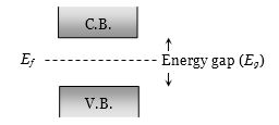
EasyMCQ
The Fermi level of energy of an intrinsic semiconductor lies:
A
In the middle of the forbidden gap
B
Below the middle of the forbidden gap
C
Above the middle of the forbidden gap
D
Outside the forbidden gap
Solution
(A) In an intrinsic semiconductor,the number of electrons in the conduction band is equal to the number of holes in the valence band. The Fermi level $(E_f)$ is defined as the energy level where the probability of finding an electron is $0.5$ at any temperature. For an intrinsic semiconductor,the Fermi level lies exactly in the middle of the forbidden energy gap $(E_g)$,midway between the top of the valence band $(E_v)$ and the bottom of the conduction band $(E_c)$. Mathematically,$E_f = (E_c + E_v) / 2$. Therefore,the correct option is $(A)$.
0 likes
View Solution22
EasyMCQ
In a semiconductor,the separation between the conduction band and the valence band is of the order of $... \, eV$.
A
$100$
B
$10$
C
$1$
D
$0$
Solution
(C) In semiconductors,the forbidden energy gap (the energy separation between the conduction band and the valence band) is typically of the order of $1 \, eV$. For example,Silicon has a band gap of approximately $1.1 \, eV$ and Germanium has a band gap of approximately $0.7 \, eV$.
0 likes
View Solution23
EasyMCQ
The intrinsic semiconductor becomes an insulator at
A
$0^\circ C$
B
$-100^\circ C$
C
$300\;K$
D
$0\;K$
Solution
(D) At $0\;K$ temperature,an intrinsic semiconductor behaves as an insulator. This is because,at absolute zero temperature,there is no thermal energy available for electrons to jump from the valence band to the conduction band. Consequently,the valence band is completely filled and the conduction band is completely empty,resulting in zero electrical conductivity.
0 likes
View Solution24
EasyMCQ
The resistance of a semiconductor at $0 \ K$ is:
A
Zero
B
Infinite
C
Large
D
Small
Solution
(B) At $0 \ K$,the valence band of a semiconductor is completely filled and the conduction band is completely empty.
There are no free charge carriers available for conduction.
Therefore,a semiconductor behaves as a perfect insulator at $0 \ K$.
Since an insulator has infinite resistance,the resistance of a semiconductor at $0 \ K$ is infinite.
There are no free charge carriers available for conduction.
Therefore,a semiconductor behaves as a perfect insulator at $0 \ K$.
Since an insulator has infinite resistance,the resistance of a semiconductor at $0 \ K$ is infinite.
0 likes
View Solution25
EasyMCQ
In a good conductor,the energy gap between the conduction band and the valence band is:
A
Infinite
B
Wide
C
Narrow
D
Zero
Solution
(D) In a good conductor,the conduction band and the valence band overlap each other.
Therefore,the energy gap between these two bands is effectively $0 \ eV$ (Zero).
Therefore,the energy gap between these two bands is effectively $0 \ eV$ (Zero).
0 likes
View Solution26
EasyMCQ
The temperature coefficient of resistance of a semiconductor is:
A
Always positive
B
Always negative
C
Zero
D
May be positive, negative, or zero
Solution
(B) In a semiconductor, as the temperature increases, the number of charge carriers (electrons and holes) increases significantly due to the thermal excitation of electrons from the valence band to the conduction band. This increase in charge carrier density outweighs the increase in scattering, leading to a decrease in electrical resistance. Since the resistance decreases as temperature increases, the temperature coefficient of resistance $(\alpha)$ is defined as $\alpha = \frac{1}{R} \frac{dR}{dT}$, which is always negative for semiconductors.
0 likes
View Solution27
EasyMCQ
In the case of a semiconductor,which of the following statements is wrong?
A
Doping increases conductivity.
B
The temperature coefficient of resistance is negative.
C
Resistivity is between that of a conductor and an insulator.
D
At absolute zero temperature,it behaves like a conductor.
Solution
(D) The correct answer is $D$.
At absolute zero temperature $(T = 0 \ K)$,all valence electrons are tightly bound in the covalent bonds of the semiconductor crystal lattice.
There are no free charge carriers available for conduction.
Therefore,at absolute zero,a semiconductor behaves as a perfect insulator,not a conductor.
At absolute zero temperature $(T = 0 \ K)$,all valence electrons are tightly bound in the covalent bonds of the semiconductor crystal lattice.
There are no free charge carriers available for conduction.
Therefore,at absolute zero,a semiconductor behaves as a perfect insulator,not a conductor.
0 likes
View Solution28
MediumMCQ
The manifestation of band structure in solids is due to
A
Boltzmann's law
B
Pauli's exclusion principle
C
Bohr's theory
D
Heisenberg's uncertainty principle
Solution
(B) The formation of energy bands in solids is a direct consequence of $Pauli's$ exclusion principle. According to this principle,no two electrons in an atom can have the same set of four quantum numbers. When atoms are brought together to form a solid,their discrete energy levels split into closely spaced energy bands due to the interaction between electrons and the requirement that each electron must occupy a unique quantum state.
0 likes
View Solution29
EasyMCQ
At ordinary temperatures, the electrical conductivity of semiconductors in $S/m$ (or $mho/m$) is in the range:
A
$10^{-3}$ to $10^{-4}$
B
$10^2$ to $10^3$
C
$10^{-6}$ to $10^{-10}$
D
$10^{-10}$ to $10^{-16}$
Solution
(B) The electrical conductivity $(\sigma)$ of materials is categorized based on their ability to conduct electricity.
Metals are good conductors with high conductivity, typically in the range of $10^6$ to $10^8 \ S/m$.
Insulators have very low conductivity, typically in the range of $10^{-10}$ to $10^{-20} \ S/m$.
Semiconductors have conductivity values intermediate between conductors and insulators, typically in the range of $10^{-6}$ to $10^4 \ S/m$ depending on the material and temperature.
Given the options provided, the range $10^2$ to $10^3 \ S/m$ is the most appropriate representation for semiconductors among the choices.
0 likes
View Solution30
EasyMCQ
When the temperature of a silicon sample is increased from $27^\circ C$ to $100^\circ C$,the conductivity of silicon will be
A
Increased
B
Decreased
C
Remain same
D
Zero
Solution
(A) Silicon is an intrinsic semiconductor. In semiconductors,the energy band gap between the valence band and the conduction band is small.
As the temperature increases,more electrons gain sufficient thermal energy to jump from the valence band to the conduction band.
This results in an increase in the number of charge carriers (both electrons and holes).
Since conductivity $\sigma$ is directly proportional to the number density of charge carriers,the conductivity of silicon increases with an increase in temperature.
0 likes
View Solution31
EasyMCQ
GaAs is
A
Element semiconductor
B
Alloy semiconductor
C
Bad conductor
D
Metallic semiconductor
Solution
(B) GaAs (Gallium Arsenide) is a compound semiconductor formed by the combination of elements from group $III$ and group $V$ of the periodic table.
These are known as compound or alloy semiconductors.
Therefore,the correct option is $B$.
These are known as compound or alloy semiconductors.
Therefore,the correct option is $B$.
0 likes
View Solution32
EasyMCQ
The state of the energy gained by valence electrons when the temperature is raised or when an electric field is applied is called as:
A
Valence band
B
Conduction band
C
Forbidden band
D
None of these
Solution
(B) When the temperature of a semiconductor is raised or an external electric field is applied,valence electrons gain sufficient energy to jump across the forbidden energy gap from the valence band to the conduction band. Once in the conduction band,these electrons are free to move through the crystal lattice,thereby contributing to electrical conduction. Therefore,the state of the energy gained by these electrons is referred to as the conduction band.
0 likes
View Solution33
EasyMCQ
For a germanium crystal,the forbidden energy gap in joules is:
A
$1.12 \times 10^{-19} \ J$
B
$1.76 \times 10^{-19} \ J$
C
$1.6 \times 10^{-19} \ J$
D
Zero
Solution
(A) The forbidden energy gap $({E_g})$ for germanium $(Ge)$ at room temperature is approximately $0.7 \ eV$.
To convert this value from electron-volts $(eV)$ to joules $(J)$,we use the conversion factor $1 \ eV = 1.6 \times 10^{-19} \ J$.
Therefore,${E_g} = 0.7 \ eV = 0.7 \times 1.6 \times 10^{-19} \ J$.
${E_g} = 1.12 \times 10^{-19} \ J$.
To convert this value from electron-volts $(eV)$ to joules $(J)$,we use the conversion factor $1 \ eV = 1.6 \times 10^{-19} \ J$.
Therefore,${E_g} = 0.7 \ eV = 0.7 \times 1.6 \times 10^{-19} \ J$.
${E_g} = 1.12 \times 10^{-19} \ J$.
0 likes
View Solution34
EasyMCQ
$A$ pure semiconductor behaves slightly as a conductor at
A
Room temperature
B
Low temperature
C
High temperature
D
Both $(b)$ and $(c)$
Solution
(A) At $0 \ K$ (absolute zero),a pure semiconductor acts as a perfect insulator because all valence electrons are tightly bound in covalent bonds.
As the temperature increases,thermal energy causes some covalent bonds to break,releasing free electrons into the conduction band and creating holes in the valence band.
At room temperature,this thermal excitation is sufficient for a small number of charge carriers to be generated,allowing the semiconductor to behave slightly as a conductor.
Therefore,the correct option is $(a)$.
0 likes
View Solution35
EasyMCQ
Which is the correct relation for the forbidden energy gap in a conductor,semiconductor,and insulator?
A
$ \Delta E_{g, \text{conductor}} > \Delta E_{g, \text{semiconductor}} > \Delta E_{g, \text{insulator}} $
B
$ \Delta E_{g, \text{insulator}} > \Delta E_{g, \text{semiconductor}} > \Delta E_{g, \text{conductor}} $
C
$ \Delta E_{g, \text{conductor}} > \Delta E_{g, \text{insulator}} > \Delta E_{g, \text{semiconductor}} $
D
$ \Delta E_{g, \text{semiconductor}} > \Delta E_{g, \text{conductor}} > \Delta E_{g, \text{insulator}} $
Solution
(B) In a conductor,the valence band and conduction band overlap,so the forbidden energy gap $\Delta E_g$ is effectively $0 \text{ eV}$.
In a semiconductor,the forbidden energy gap is small,typically around $1 \text{ eV}$ (e.g.,$1.1 \text{ eV}$ for Silicon).
In an insulator,the forbidden energy gap is very large,typically greater than $3 \text{ eV}$ to $5 \text{ eV}$.
Therefore,the correct relation is $\Delta E_{g, \text{insulator}} > \Delta E_{g, \text{semiconductor}} > \Delta E_{g, \text{conductor}}$.
0 likes
View Solution36
EasyMCQ
The band gap in Germanium and Silicon in $eV$ respectively is
A
$0.7, 1.1$
B
$1.1, 0.7$
C
$1.1, 0$
D
$0, 1.1$
Solution
(A) The energy band gap $(E_g)$ is the energy difference between the top of the valence band and the bottom of the conduction band.
For Germanium $(Ge)$,the band gap is approximately $0.7 \ eV$ at room temperature.
For Silicon $(Si)$,the band gap is approximately $1.1 \ eV$ at room temperature.
Therefore,the band gap in Germanium and Silicon respectively is $0.7 \ eV$ and $1.1 \ eV$.
For Germanium $(Ge)$,the band gap is approximately $0.7 \ eV$ at room temperature.
For Silicon $(Si)$,the band gap is approximately $1.1 \ eV$ at room temperature.
Therefore,the band gap in Germanium and Silicon respectively is $0.7 \ eV$ and $1.1 \ eV$.
0 likes
View Solution37
EasyMCQ
The valence band and conduction band of a solid overlap at low temperature. The solid may be:
A
$A$ metal
B
$A$ semiconductor
C
An insulator
D
None of these
Solution
(A) In solids,the electrical conductivity depends on the energy gap between the valence band and the conduction band.
In metals (conductors),the valence band and the conduction band overlap each other.
This overlap allows electrons to move freely from the valence band to the conduction band even at low temperatures,resulting in high electrical conductivity.
Therefore,the solid is a metal.
In metals (conductors),the valence band and the conduction band overlap each other.
This overlap allows electrons to move freely from the valence band to the conduction band even at low temperatures,resulting in high electrical conductivity.
Therefore,the solid is a metal.
0 likes
View Solution38
EasyMCQ
In a semiconductor,
A
There are no free electrons at any temperature.
B
The number of free electrons is more than that in a conductor.
C
There are no free electrons at $0 \ K$.
D
None of these.
Solution
(C) At $0 \ K$,the valence band is completely filled and the conduction band is completely empty in a semiconductor. Due to the large energy gap between the valence band and the conduction band,no electrons can jump to the conduction band at absolute zero temperature. Therefore,a semiconductor behaves as a perfect insulator at $0 \ K$.
0 likes
View Solution39
EasyMCQ
The energy band gap is maximum in
A
Metals
B
Superconductors
C
Insulators
D
Semiconductors
Solution
(C) The correct answer is $C$.
In insulators,the valence electrons are tightly bound to the nucleus.
At room temperature,the available thermal energy is insufficient to excite electrons from the valence band to the conduction band.
The energy band gap in insulators is typically large,often greater than $3 \ eV$ (usually around $6 \ eV$),which prevents electrical conduction.
In contrast,semiconductors have a small band gap (around $1 \ eV$),and metals have no band gap (the valence and conduction bands overlap).
0 likes
View Solution40
EasyMCQ
For non-conductors (insulators),the energy gap is: (in $, eV$)
A
$6$
B
$1.1$
C
$0.8$
D
$0.3$
Solution
(A) In insulators (non-conductors),the valence band and conduction band are separated by a large energy gap,typically greater than $3\, eV$.
Among the given options,$6\, eV$ is the only value that represents a typical energy gap for an insulator.
$1.1\, eV$ is characteristic of Silicon (semiconductor),while $0.8\, eV$ and $0.3\, eV$ are characteristic of other semiconductors like Germanium or specific alloys.
Therefore,the correct option is $A$.
0 likes
View Solution41
EasyMCQ
In semiconductors at room temperature,which of the following statements is correct regarding their energy bands?
A
The valence band is partially empty and the conduction band is partially filled.
B
The valence band is completely filled and the conduction band is partially filled.
C
The valence band is completely filled.
D
The conduction band is completely empty.
Solution
(A) At room temperature,thermal energy is sufficient to excite some electrons from the valence band to the conduction band in a semiconductor.
As a result,the valence band becomes partially empty (creating holes) and the conduction band becomes partially filled with these excited electrons.
Therefore,the correct statement is that the valence band is partially empty and the conduction band is partially filled.
As a result,the valence band becomes partially empty (creating holes) and the conduction band becomes partially filled with these excited electrons.
Therefore,the correct statement is that the valence band is partially empty and the conduction band is partially filled.
0 likes
View Solution42
EasyMCQ
Regarding a semiconductor,which one of the following is wrong?
A
There are no free electrons at room temperature
B
There are no free electrons at $0 \ K$
C
The number of free electrons increases with rise of temperature
D
The charge carriers are electrons and holes
Solution
(A) In a semiconductor,at room temperature,thermal energy is sufficient to break some covalent bonds,which generates electron-hole pairs. Therefore,free electrons are present at room temperature. At $0 \ K$,a semiconductor behaves as a perfect insulator because there is no thermal energy to break bonds,meaning there are no free electrons. Thus,option $A$ is incorrect.
0 likes
View Solution43
EasyMCQ
Choose the correct statement.
A
When we heat a semiconductor, its resistance increases.
B
When we heat a semiconductor, its resistance decreases.
C
When we cool a semiconductor to $0 \text{ K}$, it becomes a superconductor.
D
Resistance of a semiconductor is independent of temperature.
Solution
(B) The correct statement is that when we heat a semiconductor, its resistance decreases.
In semiconductors, the energy gap between the valence band and the conduction band is small.
As the temperature increases, more electrons gain sufficient thermal energy to jump from the valence band to the conduction band.
This increase in the number of charge carriers (electrons and holes) leads to an increase in conductivity.
Since conductivity is the reciprocal of resistivity (and resistance), an increase in conductivity implies a decrease in resistance.
0 likes
View Solution44
EasyMCQ
In extrinsic semiconductors,
A
The conduction band and valence band overlap.
B
The gap between conduction band and valence band is more than $16 \ eV$.
C
The gap between conduction band and valence band is near about $1 \ eV$.
D
The gap between conduction band and valence band will be $100 \ eV$ and more.
Solution
(C) In semiconductors,the energy gap $(E_g)$ between the valence band and the conduction band is small,typically around $1 \ eV$.
Extrinsic semiconductors are formed by doping intrinsic semiconductors (like Silicon or Germanium) with impurities.
Doping does not significantly change the band gap of the material; it only introduces new energy levels within the existing band gap.
Therefore,the energy gap remains near $1 \ eV$ for extrinsic semiconductors,similar to their intrinsic counterparts.
Thus,option $(C)$ is correct.
0 likes
View Solution45
EasyMCQ
Resistivity of a semiconductor depends on
A
Shape of semiconductor
B
Atomic nature of semiconductor
C
Length of semiconductor
D
Shape and atomic nature of semiconductor
Solution
(B) Resistivity $(\rho)$ is an intrinsic property of a material. It depends on the atomic nature of the material, such as the concentration of charge carriers and their mobility, which are determined by the atomic structure and temperature. It does not depend on the geometric dimensions like length, area of cross-section, or the shape of the semiconductor. Therefore, the correct option is $(B)$.
0 likes
View Solution46
MediumMCQ
The energy gap of silicon is $1.14 \ eV$. The maximum wavelength at which silicon will begin absorbing energy is.....$\mathring A$
A
$10888$
B
$1088.8$
C
$108.88$
D
$10.888$
Solution
(A) The energy gap $E_g$ is given as $1.14 \ eV$.
To find the maximum wavelength $\lambda_{\max}$ that can be absorbed,we use the relation $E_g = \frac{hc}{\lambda_{\max}}$.
Rearranging for $\lambda_{\max}$,we get $\lambda_{\max} = \frac{hc}{E_g}$.
Substituting the values: $h = 6.626 \times 10^{-34} \ J \cdot s$,$c = 3 \times 10^8 \ m/s$,and $E_g = 1.14 \times 1.6 \times 10^{-19} \ J$.
$\lambda_{\max} = \frac{6.626 \times 10^{-34} \times 3 \times 10^8}{1.14 \times 1.6 \times 10^{-19}} \approx 1.0888 \times 10^{-6} \ m$.
Converting to $\mathring A$: $1.0888 \times 10^{-6} \ m = 10888 \ \mathring A$.
0 likes
View Solution47
MediumMCQ
The relation between the number of free electrons in semiconductors $(n)$ and its temperature $(T)$ is
A
$n \propto T^2$
B
$n \propto T$
C
$n \propto \sqrt{T}$
D
$n \propto T^{3/2}$
Solution
(D) In an intrinsic semiconductor,the concentration of charge carriers $(n)$ is given by the relation:
$n = A T^{3/2} \exp\left(-\frac{E_g}{2 k_B T}\right)$
where $A$ is a constant,$E_g$ is the band gap energy,and $k_B$ is the Boltzmann constant.
For a small range of temperatures,the exponential term varies slowly compared to the power term $T^{3/2}$.
Therefore,the dominant temperature dependence is $n \propto T^{3/2}$.
0 likes
View Solution48
MediumMCQ
Which of the energy band diagrams shown in the figure corresponds to that of a semiconductor?
A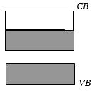
B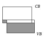
C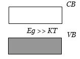
D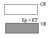
Solution
(D) In semiconductors,the forbidden energy gap $(E_g)$ between the valence band $(VB)$ and the conduction band $(CB)$ is small,typically on the order of $1 \ eV$ or comparable to the thermal energy $k_BT$.
- Diagram $A$ shows overlapping bands,which is characteristic of a conductor.
- Diagram $B$ shows a small gap,but the representation is not standard for a semiconductor.
- Diagram $C$ shows a large energy gap $(E_g \gg k_BT)$,which is characteristic of an insulator.
- Diagram $D$ shows a small energy gap $(E_g \approx k_BT)$,which is the characteristic energy band structure of a semiconductor.
Therefore,the correct diagram is $D$.
0 likes
View SolutionSemiconductor Electronics — Classification of Materials and Energy Band Theory · Frequently Asked Questions
1Are these Semiconductor Electronics questions useful for JEE and NEET?
Yes. All questions in this section are mapped to JEE Main and NEET exam patterns. Previous year questions from JEE Main, NEET, GUJCET and state-level exams are included with full solutions.
2Can I switch to Hindi or Gujarati for these questions?
Yes. Use the language tabs in the hero section or the sidebar to view the same questions and solutions in English, Hindi or Gujarati.
3How do I generate a question paper from this subtopic?
Use the Vedclass Exam Paper Generator — select the chapter and subtopic, set difficulty, and generate Sets A, B, C, D automatically. First 3 chapters of every subject are free.
Vedclass Products
For Students
Vedclass Test Series
Mock tests in real JEE/NEET style with performance analysis. 5-day free trial.
Start Free TrialFor Teachers
Exam Paper Generator
Generate Set A/B/C/D papers from this chapter in 2 minutes. 3 chapters free.
Try FreeFor Institutes
Online Exam Module
Live online exams with unlimited students, 360° analytics & white-label branding.
See DemoFor Teachers & Institutes
Generate a Semiconductor Electronics Exam Paper in 2 Minutes
Select subtopic & difficulty — Sets A, B, C, D auto-generated with No Repeat logic.
First 3 chapters of every subject are free — no payment required.