
A English
PN Junction and Diode Questions in English
Class 12 Physics · Semiconductor Electronics · PN Junction and Diode
404+
Questions
English
Language
100%
With Solutions
Showing 50 of 404 questions in English
301
MediumMCQ
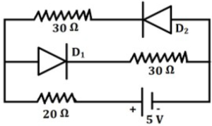
If the internal resistance of the cell is negligible,then the current flowing through the circuit is: (in $A$)
A
$0.04$
B
$0.06$
C
$0.08$
D
$0.10$
Solution
(D) In the given circuit,the diode $D_1$ is forward-biased because its p-side is connected to the positive terminal of the battery. The diode $D_2$ is reverse-biased because its p-side is connected to the negative terminal of the battery.
Therefore,no current flows through the branch containing $D_2$.
The circuit effectively consists of the battery $(5 \ V)$,the resistor $(20 \ \Omega)$,and the branch containing $D_1$ with a resistor $(30 \ \Omega)$ in series.
The total resistance of the circuit is $R_{eq} = 20 \ \Omega + 30 \ \Omega = 50 \ \Omega$.
Using Ohm's law,the current $I$ flowing through the circuit is $I = \frac{V}{R_{eq}} = \frac{5 \ V}{50 \ \Omega} = 0.1 \ A$.
0 likes
View Solution302
EasyMCQ
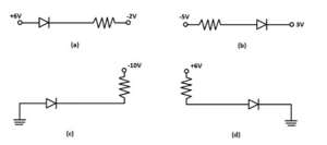
In which of the following figures is the $p-n$ junction diode reverse biased?
A
$(c)$
B
$(d)$
C
$(b)$
D
$(a)$
Solution
(C) $p-n$ junction diode is reverse biased when the $p$-terminal (anode) is at a lower potential than the $n$-terminal (cathode).
Let us analyze each figure:
$(a)$ $p$-side is at $+6 \text{ V}$,$n$-side is at $-2 \text{ V}$. Since $V_p > V_n$,it is forward biased.
$(b)$ $p$-side is at $-5 \text{ V}$,$n$-side is at $+3 \text{ V}$. Since $V_p < V_n$,it is reverse biased.
$(c)$ $p$-side is at $0 \text{ V}$ (ground),$n$-side is at $-10 \text{ V}$. Since $V_p > V_n$,it is forward biased.
$(d)$ $p$-side is at $+6 \text{ V}$,$n$-side is at $0 \text{ V}$ (ground). Since $V_p > V_n$,it is forward biased.
Therefore,the diode in figure $(b)$ is reverse biased.
0 likes
View Solution303
EasyMCQ
When a forward bias is applied to a $p-n$ junction,what happens to the potential barrier?
A
increases
B
decreases
C
remains unchanged
D
becomes zero
Solution
(B) In a $p-n$ junction,the potential barrier is created by the depletion region,which opposes the flow of majority charge carriers.
When a forward bias is applied,the positive terminal of the battery is connected to the $p$-side and the negative terminal to the $n$-side.
This external electric field opposes the internal electric field of the depletion region.
As a result,the width of the depletion region decreases,which leads to a reduction in the potential barrier height.
Therefore,the potential barrier decreases.
0 likes
View Solution304
EasyMCQ
If a $p-n$ junction diode is forward biased,then:
A
electric conduction is not possible.
B
width of depletion layer decreases.
C
width of depletion layer increases.
D
barrier voltage increases.
Solution
(B) When a $p-n$ junction diode is forward biased,the positive terminal of the external battery is connected to the $p$-side and the negative terminal to the $n$-side.
This configuration pushes the holes in the $p$-region and electrons in the $n$-region towards the junction.
As a result,the majority charge carriers move towards the junction,which effectively reduces the width of the depletion layer.
Consequently,the potential barrier height decreases,allowing current to flow easily through the diode.
0 likes
View Solution305
EasyMCQ
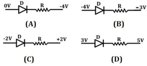
Which of the following figures represents a forward-biased diode?
A
$A$
B
$B$
C
$C$
D
$D$
Solution
(A) diode is forward-biased when the potential at the $p$-side (anode) is higher than the potential at the $n$-side (cathode).
In the given circuits,the triangle represents the $p$-side and the vertical bar represents the $n$-side.
For option $A$: $V_p = 0 \ V$,$V_n = -4 \ V$. Since $0 \ V > -4 \ V$,the diode is forward-biased.
For option $B$: $V_p = -4 \ V$,$V_n = -3 \ V$. Since $-4 \ V < -3 \ V$,the diode is reverse-biased.
For option $C$: $V_p = -2 \ V$,$V_n = +2 \ V$. Since $-2 \ V < +2 \ V$,the diode is reverse-biased.
For option $D$: $V_p = 3 \ V$,$V_n = 5 \ V$. Since $3 \ V < 5 \ V$,the diode is reverse-biased.
Therefore,the correct figure is $A$.
0 likes
View Solution306
EasyMCQ
The potential barrier in a $p-n$ junction diode is due to
A
depletion of positive charges near the junction.
B
accumulation of positive charges near the junction.
C
depletion of negative charges near the junction.
D
accumulation of positive and negative charges near the junction.
Solution
(D) When a $p-n$ junction is formed,electrons from the $n$-region diffuse into the $p$-region,and holes from the $p$-region diffuse into the $n$-region.
This diffusion leaves behind immobile ionized donor atoms (positive charges) in the $n$-side and immobile ionized acceptor atoms (negative charges) in the $p$-side near the junction.
This region,which is devoid of mobile charge carriers,is called the depletion region.
The accumulation of these fixed positive and negative charges creates an electric field that opposes further diffusion,resulting in a potential barrier.
0 likes
View Solution307
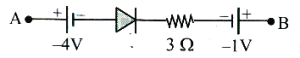
EasyMCQ
Find the magnitude of current in the given circuit. (in $A$)
A
$0$
B
$1$
C
$0.1$
D
$0.2$
Solution
(A) In the given circuit,the $p$-terminal of the diode is connected to the negative terminal of the $4 \ V$ battery,and the $n$-terminal is connected towards the $1 \ V$ battery.
Specifically,the potential at the $p$-side is $-4 \ V$ and the potential at the $n$-side is $-1 \ V$.
Since the potential at the $p$-side is lower than the potential at the $n$-side $(-4 \ V < -1 \ V)$,the diode is in a reverse-biased condition.
An ideal diode in reverse bias acts as an open circuit,meaning it offers infinite resistance.
Therefore,no current will flow through the circuit.
The magnitude of the current is $0 \ A$.
0 likes
View Solution308
EasyMCQ
$A$ semiconductor device $X$ is connected in series with a battery and a resistor. $A$ current of $10 \ mA$ is found to pass through the circuit. If the terminals of $X$ are connected in reverse,the current drops to almost zero. $X$ may be
A
a zener diode
B
a p-n junction diode
C
an intrinsic semiconductor
D
an extrinsic semiconductor
Solution
(B) $p-n$ junction diode allows current to flow easily when it is forward biased.
When the terminals are reversed,the diode becomes reverse biased.
In a reverse biased state,the depletion region widens,offering very high resistance to the flow of charge carriers.
Consequently,the current drops to almost zero.
Therefore,the device $X$ is a $p-n$ junction diode.
When the terminals are reversed,the diode becomes reverse biased.
In a reverse biased state,the depletion region widens,offering very high resistance to the flow of charge carriers.
Consequently,the current drops to almost zero.
Therefore,the device $X$ is a $p-n$ junction diode.
0 likes
View Solution309
EasyMCQ
The depletion layer in $p-n$ junction region is caused by
A
drift of electrons.
B
migration of impurity ions.
C
diffusion of charge carriers.
D
drift of holes.
Solution
(C) The correct option is $C$.
When a $p-n$ junction is formed,there is a high concentration of electrons in the $n$-region and a high concentration of holes in the $p$-region.
Due to this concentration gradient,electrons diffuse from the $n$-side to the $p$-side,and holes diffuse from the $p$-side to the $n$-side.
As these charge carriers cross the junction,they recombine near the junction interface.
This recombination leaves behind immobile ionized impurity atoms (positive ions on the $n$-side and negative ions on the $p$-side),which create an electric field that opposes further diffusion.
This region,depleted of mobile charge carriers,is known as the depletion layer.
0 likes
View Solution310
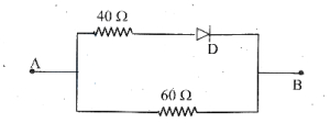
MediumMCQ
For the diagram shown,the resistance between points $A$ and $B$ when the ideal diode '$D$' is forward biased is '$R_1$' and that when reverse biased is '$R_2$'. The ratio $\frac{R_1}{R_2}$ is
A
$\frac{2}{3}$
B
$\frac{2}{5}$
C
$\frac{3}{2}$
D
$\frac{5}{2}$
Solution
(B) When the diode is forward biased,it acts as a short circuit (zero resistance). The two resistors $40 \ \Omega$ and $60 \ \Omega$ are in parallel.
$\therefore$ The effective resistance $R_1$ is given by:
$R_1 = \frac{40 \times 60}{40 + 60} = \frac{2400}{100} = 24 \ \Omega$
When the diode is reverse biased,it acts as an open circuit (infinite resistance). No current flows through the upper branch.
$\therefore$ The effective resistance $R_2$ is simply the resistance of the lower branch,which is $60 \ \Omega$.
$\therefore \frac{R_1}{R_2} = \frac{24}{60} = \frac{2}{5}$
0 likes
View Solution311
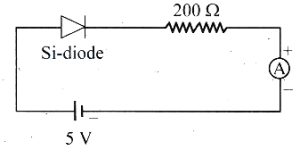
EasyMCQ
In the following circuit,the reading in the ammeter is (in $mA$)
A
$25.1$
B
$22.5$
C
$21.5$
D
$21.25$
Solution
(C) The reading of the ammeter represents the current flowing through the circuit.
According to Ohm's law for a circuit containing a diode,the current $I$ is given by:
$I = \frac{V - V_{\text{diode}}}{R}$
Here,the supply voltage $V = 5 \text{ V}$,the resistance $R = 200 \text{ } \Omega$,and for a silicon diode,the forward voltage drop $V_{\text{diode}} = 0.7 \text{ V}$.
Substituting these values into the formula:
$I = \frac{5 \text{ V} - 0.7 \text{ V}}{200 \text{ } \Omega}$
$I = \frac{4.3 \text{ V}}{200 \text{ } \Omega} = 0.0215 \text{ A}$
Converting the current to milliamperes $(1 \text{ A} = 1000 \text{ mA})$:
$I = 0.0215 \times 1000 \text{ mA} = 21.5 \text{ mA}$
Thus,the reading in the ammeter is $21.5 \text{ mA}$.
0 likes
View Solution312
EasyMCQ
Two ideal diodes are connected to a battery as shown in the circuit. The current supplied by the battery is
A
zero
B
$0.25$ $A$
C
$0.50$ $A$
D
$0.75$ $A$
Solution
(B) In the given circuit,the diode $D_2$ is connected in reverse bias because its $n$-terminal is connected to the positive terminal of the battery.
Therefore,no current flows through the branch containing the $40 \Omega$ resistor.
The circuit simplifies to a single loop with the $40 \Omega$ resistor and the diode $D_1$ in forward bias.
Using Ohm's law,the current $I$ supplied by the battery is $I = \frac{V}{R} = \frac{10 \text{ V}}{40 \Omega} = 0.25 \text{ A}$.
0 likes
View Solution313
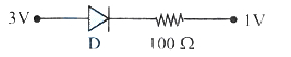
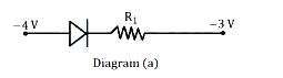
EasyMCQ
Assuming that the junction diode is ideal, find the current in the arrangement shown in the figure. (in $\text{mA}$)
A
$2$
B
$20$
C
$30$
D
$10$
Solution
(B) For the given circuit, the diode is forward-biased because the potential at the anode $(3 \text{ V})$ is higher than the potential at the cathode $(1 \text{ V})$.
Since the diode is ideal, its resistance in the forward-biased state is $0 \Omega$.
The potential difference across the resistor is $\Delta V = 3 \text{ V} - 1 \text{ V} = 2 \text{ V}$.
Using Ohm's law, the current $i$ flowing through the circuit is:
$i = \frac{\Delta V}{R} = \frac{2 \text{ V}}{100 \Omega} = 0.02 \text{ A}$.
Converting this to milliamperes:
$i = 0.02 \times 1000 \text{ mA} = 20 \text{ mA}$.
Since the diode is ideal, its resistance in the forward-biased state is $0 \Omega$.
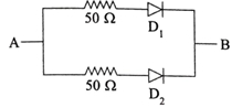
The potential difference across the resistor is $\Delta V = 3 \text{ V} - 1 \text{ V} = 2 \text{ V}$.
Using Ohm's law, the current $i$ flowing through the circuit is:
$i = \frac{\Delta V}{R} = \frac{2 \text{ V}}{100 \Omega} = 0.02 \text{ A}$.
Converting this to milliamperes:
$i = 0.02 \times 1000 \text{ mA} = 20 \text{ mA}$.
0 likes
View Solution314
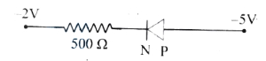
EasyMCQ
What is the current in the following junction diode circuit?
A
$10^{-1} \text{ A}$
B
zero
C
$10^{-2} \text{ A}$
D
$5 \times 10^{-3} \text{ A}$
Solution
(B) In the given circuit,the $P$-terminal of the diode is connected to $-5 \text{ V}$ and the $N$-terminal is connected to $-2 \text{ V}$ through a resistor.
For a diode to be forward biased,the potential at the $P$-terminal must be higher than the potential at the $N$-terminal.
Here,the potential at the $P$-terminal $(V_P = -5 \text{ V})$ is less than the potential at the $N$-terminal $(V_N = -2 \text{ V})$.
Since $V_P < V_N$,the diode is in reverse bias.
In an ideal diode,no current flows in reverse bias. Therefore,the current in the circuit is zero.
0 likes
View Solution315
EasyMCQ
If the $p-n$ junction diode is unbiased,
A
$n$-type side has lower potential than $p$-type side.
B
$n$-type side has same potential as $p$-type side.
C
An electric field is established at the junction such that $n$-side is at positive voltage relative to $p$-side.
D
The potential across the junction is such that $p$-side is at positive voltage relative to $n$-side.
Solution
(A) When a $p-n$ junction is formed,electrons diffuse from the $n$-region to the $p$-region,and holes diffuse from the $p$-region to the $n$-region.
This diffusion creates a depletion region with a built-in electric field directed from the $n$-side to the $p$-side.
Due to this electric field,the $p$-side acquires a higher potential relative to the $n$-side.
Therefore,the $n$-type side has a lower potential than the $p$-type side.
This diffusion creates a depletion region with a built-in electric field directed from the $n$-side to the $p$-side.
Due to this electric field,the $p$-side acquires a higher potential relative to the $n$-side.
Therefore,the $n$-type side has a lower potential than the $p$-type side.
0 likes
View Solution316
EasyMCQ
In the reverse biasing of a $p-n$ junction diode,
A
the width of the depletion layer decreases.
B
the width of the depletion layer increases.
C
the number of minority charge carriers increase.
D
the number of majority charge carriers increase.
Solution
(B) When a $p-n$ junction diode is reverse biased,the positive terminal of the battery is connected to the $n$-region and the negative terminal to the $p$-region.
This configuration pulls the majority charge carriers (holes in $p$-region and electrons in $n$-region) away from the junction.
As a result,the depletion layer is depleted of charge carriers even further,causing its width to increase.
Therefore,the correct option is $B$.
This configuration pulls the majority charge carriers (holes in $p$-region and electrons in $n$-region) away from the junction.
As a result,the depletion layer is depleted of charge carriers even further,causing its width to increase.
Therefore,the correct option is $B$.
0 likes
View Solution317
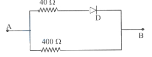
MediumMCQ
For the diagram shown,the resistances between points $A$ and $B$ when the ideal diode $D$ is forward biased is $R_1$ and when it is reverse biased is $R_2$. The ratio $R_1: R_2$ is
A
$2: 1$
B
$1: 1$
C
$1: 2$
D
$1: 11$
Solution
(D) When the diode $D$ is forward biased,it acts as a short circuit (zero resistance). The circuit consists of two resistors of $40 \ \Omega$ and $400 \ \Omega$ in parallel.
Therefore,the effective resistance $R_1$ is given by:
$R_1 = \frac{40 \times 400}{40 + 400} = \frac{16000}{440} = \frac{1600}{44} = \frac{400}{11} \ \Omega$
When the diode $D$ is reverse biased,it acts as an open circuit (infinite resistance). No current flows through the upper branch.
Therefore,the effective resistance $R_2$ is simply the resistance of the lower branch:
$R_2 = 400 \ \Omega$
Now,calculating the ratio $R_1: R_2$:
$\frac{R_1}{R_2} = \frac{400/11}{400} = \frac{1}{11}$
Thus,the ratio $R_1: R_2$ is $1: 11$.
0 likes
View Solution318
EasyMCQ
If a $p-n$ junction diode is in forward bias,then:
A
width of depletion layer increases
B
electric conduction is not possible at all
C
barrier voltage increases
D
width of depletion layer decreases
Solution
(D) In a $p-n$ junction diode,when it is in forward bias,the positive terminal of the battery is connected to the $p$-region and the negative terminal to the $n$-region.
This external electric field opposes the internal barrier electric field.
As a result,the majority charge carriers are pushed towards the junction,which reduces the width of the depletion layer.
Therefore,the barrier potential decreases,allowing current to flow easily through the diode.
This external electric field opposes the internal barrier electric field.
As a result,the majority charge carriers are pushed towards the junction,which reduces the width of the depletion layer.
Therefore,the barrier potential decreases,allowing current to flow easily through the diode.
0 likes
View Solution319
EasyMCQ
When forward bias is applied to a $p-n$ junction,then what happens to the potential barrier $(V_B)$ and the width $(X)$ of the depletion region?
A
$V_B$ increases,$X$ decreases
B
$V_B$ decreases,$X$ increases
C
$V_B$ increases,$X$ increases
D
$V_B$ decreases,$X$ decreases
Solution
(D) When a $p-n$ junction is forward biased,the positive terminal of the external battery is connected to the $p$-type region and the negative terminal to the $n$-type region.
This external electric field opposes the internal electric field of the depletion region.
As a result,the effective potential barrier $(V_B)$ decreases.
Due to the reduction in the potential barrier,the majority charge carriers are pushed towards the junction,which causes the width $(X)$ of the depletion region to decrease.
Therefore,both the potential barrier and the width of the depletion region decrease.
0 likes
View Solution320
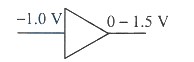
EasyMCQ
In which figure,the junction diode is forward biased?
A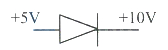
B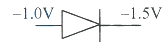
C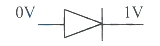
D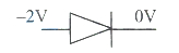
Solution
(B) junction diode is forward biased when the potential at the $P$-terminal $(V_P)$ is higher than the potential at the $N$-terminal $(V_N)$,i.e.,$V_P > V_N$.
Let us analyze each option:
$A$: $V_P = +5 \ V$,$V_N = +10 \ V$. Here $V_P < V_N$,so it is reverse biased.
$B$: $V_P = -1.0 \ V$,$V_N = -1.5 \ V$. Here $V_P > V_N$ (since $-1.0 > -1.5$),so it is forward biased.
$C$: $V_P = 0 \ V$,$V_N = +1 \ V$. Here $V_P < V_N$,so it is reverse biased.
$D$: $V_P = -2 \ V$,$V_N = 0 \ V$. Here $V_P < V_N$,so it is reverse biased.
Therefore,the correct option is $B$.
0 likes
View Solution321
EasyMCQ
On increasing the reverse bias to a large value in a $P-N$ junction diode,current
A
increase slowly.
B
remains fixed.
C
suddenly increases.
D
decreases slowly.
Solution
(C) In a $P-N$ junction diode,when the reverse bias voltage is increased to a large value,it eventually reaches the breakdown voltage.
At this point,the covalent bonds in the crystal lattice break,leading to a rapid generation of charge carriers.
Consequently,the current through the diode suddenly increases.
At this point,the covalent bonds in the crystal lattice break,leading to a rapid generation of charge carriers.
Consequently,the current through the diode suddenly increases.
0 likes
View Solution322
EasyMCQ
In a forward bias arrangement of a $p-n$ junction diode,the
A
$p$-region is connected to the positive terminal of the battery.
B
$n$-region is connected to the positive terminal of the battery.
C
$p$-region is connected to the negative terminal of the battery.
D
$n$-region is connected to the negative terminal of the battery.
Solution
(A) In a $p-n$ junction diode,forward bias occurs when the $p$-type semiconductor is connected to the positive terminal of the external battery and the $n$-type semiconductor is connected to the negative terminal.
This configuration reduces the width of the depletion layer and lowers the potential barrier,allowing current to flow easily through the diode.
This configuration reduces the width of the depletion layer and lowers the potential barrier,allowing current to flow easily through the diode.
0 likes
View Solution323
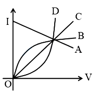
DifficultMCQ
Which one of the following graphs represents the forward bias characteristic of a diode?
A
$C$
B
$B$
C
$D$
D
$A$
Solution
(C) The forward bias characteristic of a $PN$ junction diode is non-linear and exponential in nature.
As the forward voltage $V$ increases,the current $I$ increases slowly at first and then rises rapidly after the knee voltage.
Among the given curves,curve $D$ shows an exponential increase in current with voltage,which is characteristic of the forward bias region of a diode.
Curve $A$ represents a linear decrease,$B$ represents a slow linear increase,and $C$ represents a linear increase.
Therefore,graph $D$ correctly represents the forward bias characteristic.
0 likes
View Solution324
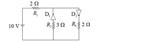
MediumMCQ
The given circuit has two ideal diodes $D_1$ and $D_2$ connected as shown in the figure. The current flowing through the resistance $R_1$ will be (in $\,A$)
A
$2$
B
$3.3$
C
$2.5$
D
$7$
Solution
(C) In the given circuit, the $10 \,V$ source is connected to the circuit.
Looking at the orientation of the diodes:
- Diode $D_1$ has its cathode connected to the positive potential side (through $R_1$), making it reverse-biased. Thus, $D_1$ acts as an open circuit (no current flows through $R_2$).
- Diode $D_2$ has its anode connected to the positive potential side, making it forward-biased. Thus, $D_2$ acts as a closed switch (short circuit).
Therefore, the circuit simplifies to a series combination of the $10 \,V$ battery, resistor $R_1 = 2 \,\Omega$, and resistor $R_3 = 2 \,\Omega$.
The total resistance in the circuit is $R_{eq} = R_1 + R_3 = 2 \,\Omega + 2 \,\Omega = 4 \,\Omega$.
The current flowing through $R_1$ is given by Ohm's law: $I = \frac{V}{R_{eq}} = \frac{10 \,V}{4 \,\Omega} = 2.5 \,A$.
0 likes
View Solution325
EasyMCQ
When a reverse bias is applied to a $p-n$ junction diode,what happens to the potential barrier?
A
It increases the minority charge carriers.
B
It lowers the potential barrier.
C
It decreases the majority charge carriers.
D
It raises the potential barrier.
Solution
(D) When a $p-n$ junction diode is reverse biased,the positive terminal of the battery is connected to the $n$-region and the negative terminal to the $p$-region.
This configuration pulls the majority charge carriers (electrons in the $n$-region and holes in the $p$-region) away from the junction.
As a result,the width of the depletion layer increases.
Because the depletion layer width increases,the potential barrier height also increases,making it more difficult for majority charge carriers to cross the junction.
0 likes
View Solution326
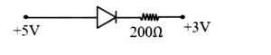
EasyMCQ
The current in the following circuit is:
A
$10 \ A$
B
zero
C
$0.025 \ A$
D
$10^{-2} \ A$
Solution
(D) The diode is connected such that the p-side is at $+5 \ V$ and the n-side is at $+3 \ V$.
Since the potential at the p-side is higher than the potential at the n-side,the diode is forward-biased.
Assuming an ideal diode,the potential difference across the resistor is $V = 5 \ V - 3 \ V = 2 \ V$.
The resistance $R$ is $200 \ \Omega$.
Using Ohm's law,the current $I$ is given by $I = \frac{V}{R} = \frac{2 \ V}{200 \ \Omega} = 0.01 \ A = 10^{-2} \ A$.
0 likes
View Solution327
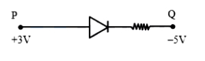
MediumMCQ
In an ideal junction diode, the current flowing through $PQ$ is (resistance is $2 \text{ k}\Omega$).
A
$2 \times 10^{-3} \text{ A}$
B
$2 \times 10^{-2} \text{ A}$
C
$4 \times 10^{-3} \text{ A}$
D
$10^{-3} \text{ A}$
Solution
(C) The diode is connected in forward bias because the $p$-side is at a higher potential $(+3 \text{ V})$ than the $n$-side $(-5 \text{ V})$.
For an ideal junction diode in forward bias, the resistance of the diode is zero.
The potential difference across the resistor is $V = V_P - V_Q = 3 \text{ V} - (-5 \text{ V}) = 8 \text{ V}$.
The resistance $R = 2 \text{ k}\Omega = 2000 \text{ }\Omega$.
Using Ohm's law, the current $I$ is given by $I = \frac{V}{R} = \frac{8 \text{ V}}{2000 \text{ }\Omega} = 4 \times 10^{-3} \text{ A}$.
0 likes
View Solution328
DifficultMCQ
Two identical ideal diodes are connected to an ammeter and a $1 \ V$ d.c. source as shown. In which one of the following circuits will the ammeter not show any deflection?
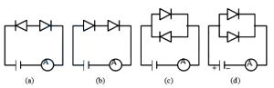
A
$(a)$
B
$(b)$
C
$(c)$
D
$(d)$
Solution
(B) In circuit $(a)$,the two diodes are connected in series such that they oppose each other. Specifically,one diode is forward-biased while the other is reverse-biased. Since an ideal reverse-biased diode acts as an open circuit (infinite resistance),no current flows through the circuit. Therefore,the ammeter will not show any deflection.
In circuit $(b)$,both diodes are forward-biased,allowing current to flow.
In circuits $(c)$ and $(d)$,the diodes are in parallel,and at least one path is forward-biased,allowing current to flow.
In circuit $(b)$,both diodes are forward-biased,allowing current to flow.
In circuits $(c)$ and $(d)$,the diodes are in parallel,and at least one path is forward-biased,allowing current to flow.
0 likes
View Solution329
DifficultMCQ
What are the values of the currents flowing in each of the following diode circuits $X$ and $Y$ respectively? (Assume that the diodes are ideal)
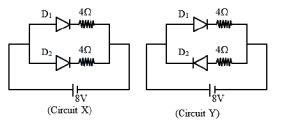
A
$1 \ A, 2 \ A$
B
$2 \ A, 1 \ A$
C
$4 \ A, 2 \ A$
D
$2 \ A, 4 \ A$
Solution
(C) In circuit $X$,both diodes $D_1$ and $D_2$ are forward biased,so both conduct current.
The two resistors of $4 \ \Omega$ each are connected in parallel.
The equivalent resistance $R_{eq}$ is given by $\frac{1}{R_{eq}} = \frac{1}{4} + \frac{1}{4} = \frac{2}{4} = \frac{1}{2}$,so $R_{eq} = 2 \ \Omega$.
The total current $I_X = \frac{V}{R_{eq}} = \frac{8 \ V}{2 \ \Omega} = 4 \ A$.
In circuit $Y$,diode $D_1$ is forward biased,but diode $D_2$ is reverse biased.
Therefore,only diode $D_1$ conducts current.
The effective resistance in the circuit is $4 \ \Omega$.
The total current $I_Y = \frac{V}{R} = \frac{8 \ V}{4 \ \Omega} = 2 \ A$.
Thus,the currents are $4 \ A$ and $2 \ A$ respectively.
0 likes
View Solution330
EasyMCQ
The region near the junction of an unbiased $p-n$ junction diode is known as the depletion layer. This layer is depleted of
A
only negative ions.
B
electrons and holes.
C
both positive and negative ions.
D
only positive ions.
Solution
(B) In an unbiased $p-n$ junction,the diffusion of electrons from the $n$-region to the $p$-region and holes from the $p$-region to the $n$-region occurs near the junction.
When these charge carriers cross the junction,they recombine and neutralize each other.
As a result,the region near the junction becomes devoid of mobile charge carriers (free electrons and holes).
This region is called the depletion layer or depletion region.
Therefore,the layer is depleted of mobile charge carriers,which are electrons and holes.
0 likes
View Solution331
Easy
In the circuit shown in the figure,the non-zero potential difference across diode $D_{1}$ and that across diode $D_{2}$ are equal. Are the diodes identical in characteristics? Explain.
Solution
(D) In the given circuit,the two diodes $D_{1}$ and $D_{2}$ are connected in series with a $DC$ voltage source.
For the circuit to conduct,both diodes must be forward-biased.
However,looking at the orientation of the diodes,$D_{1}$ is forward-biased while $D_{2}$ is reverse-biased.
In a series circuit,the current $I$ is the same through all components.
Since $D_{2}$ is reverse-biased,it offers a very high resistance,effectively acting as an open switch.
Consequently,the entire potential difference of the battery appears across the reverse-biased diode $D_{2}$,while the potential difference across the forward-biased diode $D_{1}$ is negligible (approximately $0.7 \ V$ for Silicon).
If the potential differences across $D_{1}$ and $D_{2}$ are stated to be equal,it implies that the circuit configuration or the assumption of identical characteristics must be re-evaluated,or the diodes are operating in a specific breakdown region. Given the standard interpretation,the potential difference across a reverse-biased diode is much larger than that across a forward-biased one.
0 likes
View Solution332
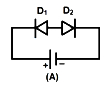
EasyMCQ
The figure shows two diagrams in which a diode and a resistance are connected. Out of the following statements,which one is $TRUE$?
A
Diagram $(A)$ and diagram $(B)$ both are forward biased.
B
Diagram $(A)$ is forward biased and diagram $(B)$ is reverse biased.
C
Diagram $(A)$ and diagram $(B)$ both are reverse biased.
D
Diagram $(A)$ is reverse biased and diagram $(B)$ is forward biased.
Solution
(D) In a $PN$ junction diode,the diode is forward biased if the potential at the anode (p-side) is higher than the potential at the cathode (n-side). It is reverse biased if the potential at the anode is lower than the potential at the cathode.
In diagram $(A)$,the anode is at $-4 \ V$ and the cathode is at $-3 \ V$. Since $-4 \ V < -3 \ V$,the anode is at a lower potential than the cathode,so diagram $(A)$ is reverse biased.
In diagram $(B)$,assuming the standard configuration where the anode is at $-2 \ V$ and the cathode is at $-4 \ V$ (based on typical textbook problems of this type),the anode is at a higher potential than the cathode,so diagram $(B)$ is forward biased.
Therefore,diagram $(A)$ is reverse biased and diagram $(B)$ is forward biased.
0 likes
View Solution333
EasyMCQ
For an ideal diode,the current in the following arrangement is:
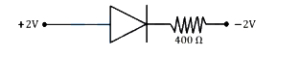
A
$10 A$
B
$10 mA$
C
$20 mA$
D
$1 mA$
Solution
(B) In the given circuit,the $p$-side of the diode is connected to $+2 V$ and the $n$-side is connected to $-2 V$ through a $400 \Omega$ resistor.
Since the potential of the $p$-side is higher than the potential of the $n$-side,the diode is forward biased.
For an ideal diode,the forward resistance is $0 \Omega$.
Therefore,the total resistance in the circuit is $R = 400 \Omega$.
The potential difference across the circuit is $V = 2 V - (-2 V) = 4 V$.
Using Ohm's law,the current $I$ is given by $I = V / R$.
$I = 4 V / 400 \Omega = 1 / 100 A = 0.01 A$.
Converting to milliamperes,$I = 0.01 \times 1000 mA = 10 mA$.
0 likes
View Solution334
EasyMCQ
The width of the depletion layer of a $p-n$ junction diode,when it is $(i)$ forward biased and $(ii)$ reverse biased,respectively,is:
A
increases and increases.
B
decreases and decreases.
C
increases and decreases.
D
decreases and increases.
Solution
(D) $(i)$ When a $p-n$ junction is forward biased,the external electric field opposes the internal electric field of the depletion region. This reduces the potential barrier and consequently decreases the width of the depletion layer.
$(ii)$ When a $p-n$ junction is reverse biased,the external electric field supports the internal electric field of the depletion region. This increases the potential barrier and consequently increases the width of the depletion layer.
$(ii)$ When a $p-n$ junction is reverse biased,the external electric field supports the internal electric field of the depletion region. This increases the potential barrier and consequently increases the width of the depletion layer.
0 likes
View Solution335
EasyMCQ
If $p-n$ junction diode is reverse biased,then:
A
potential barrier decreases.
B
width of the depletion layer decreases.
C
electrical conduction is possible.
D
width of the depletion layer increases.
Solution
(D) When a $p-n$ junction diode is reverse biased,the positive terminal of the battery is connected to the $n$-region and the negative terminal to the $p$-region.
This configuration pulls the majority charge carriers away from the junction.
As a result,the width of the depletion layer increases.
Consequently,the potential barrier also increases,which opposes the flow of current,making electrical conduction negligible.
This configuration pulls the majority charge carriers away from the junction.
As a result,the width of the depletion layer increases.
Consequently,the potential barrier also increases,which opposes the flow of current,making electrical conduction negligible.
0 likes
View Solution336
EasyMCQ
When a $p-n$ junction diode is reverse biased,then the width of the depletion layer will
A
increase and it will offer more resistance.
B
decrease and it will offer zero resistance.
C
remain constant and it will not offer resistance.
D
decrease and it will offer more resistance.
Solution
(A) In a $p-n$ junction diode,when reverse bias is applied,the positive terminal of the battery is connected to the $n$-region and the negative terminal to the $p$-region.
This causes the majority charge carriers (electrons in $n$-region and holes in $p$-region) to move away from the junction.
As a result,the depletion layer widens,and the barrier potential increases.
Due to the increased width of the depletion layer,the flow of majority charge carriers is blocked,which means the diode offers high resistance to the current.
0 likes
View Solution337
EasyMCQ
In the case of a $p-n$ junction diode,the width of the depletion region is:
A
Decreased with heavy doping
B
Increased by reverse biasing
C
Decreased with light doping
D
Increased by forward biasing
Solution
(B) In a $p-n$ junction diode,when it is reverse biased,the applied voltage supports the barrier potential,which causes the width of the depletion region to increase.
In forward biasing,the width of the depletion region decreases because the forward voltage opposes the potential barrier.
Additionally,the width of the depletion region decreases with heavy doping because the increased concentration of charge carriers leads to a narrower space charge region.
In forward biasing,the width of the depletion region decreases because the forward voltage opposes the potential barrier.
Additionally,the width of the depletion region decreases with heavy doping because the increased concentration of charge carriers leads to a narrower space charge region.
0 likes
View Solution338
MediumMCQ
Assuming that the junction diode is ideal, the current in the arrangement shown in the figure is: (in $\text{mA}$)
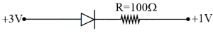
A
$30$
B
$40$
C
$20$
D
$10$
Solution
(C) The diode is connected in forward bias because the $p$-side is at $+3 \text{ V}$ and the $n$-side is at $+1 \text{ V}$.
Since the diode is ideal, its resistance in forward bias is zero.
The potential difference across the resistor $R = 100 \ \Omega$ is $V = 3 \text{ V} - 1 \text{ V} = 2 \text{ V}$.
Using Ohm's law, the current $I$ is given by $I = \frac{V}{R} = \frac{2 \text{ V}}{100 \ \Omega} = 0.02 \text{ A}$.
Converting to milliamperes, $I = 0.02 \times 1000 \text{ mA} = 20 \text{ mA}$.
0 likes
View Solution339
EasyMCQ
With forward bias mode,the $p-n$ junction diode
A
is one in which width of depletion layer increases
B
is one in which potential barrier increases
C
acts as closed switch
D
acts as open switch
Solution
(C) When a $p-n$ junction is in forward bias,the positive terminal of the battery is connected to the $p$-side and the negative terminal to the $n$-side.
This reduces the width of the depletion layer and lowers the potential barrier.
As a result,the diode offers very low resistance and allows current to flow through it.
Therefore,in forward bias,the $p-n$ junction diode acts as a closed switch.
This reduces the width of the depletion layer and lowers the potential barrier.
As a result,the diode offers very low resistance and allows current to flow through it.
Therefore,in forward bias,the $p-n$ junction diode acts as a closed switch.
0 likes
View Solution340
EasyMCQ
In a reverse-biased $pn$-junction diode,the depletion layer width:
A
decreases
B
increases
C
remains the same
D
cannot be predicted
Solution
(B) When a $pn$-junction diode is reverse-biased,the positive terminal of the external battery is connected to the $n$-region and the negative terminal to the $p$-region.
This configuration pulls the majority charge carriers (holes in the $p$-region and electrons in the $n$-region) away from the junction.
As a result,the concentration of immobile ions near the junction increases,which causes the depletion layer width to increase.
This configuration pulls the majority charge carriers (holes in the $p$-region and electrons in the $n$-region) away from the junction.
As a result,the concentration of immobile ions near the junction increases,which causes the depletion layer width to increase.
0 likes
View Solution341
EasyMCQ
If the forward voltage in a diode is increased,the width of the depletion region $\qquad$ .
A
fluctuates
B
no change
C
decreases
D
increases
Solution
(C) When a diode is forward biased,the positive terminal of the battery is connected to the $p$-type region and the negative terminal to the $n$-type region.
This external electric field opposes the internal electric field of the depletion region.
As the forward voltage increases,the potential barrier is lowered,and the majority charge carriers are pushed towards the junction.
This results in a reduction of the width of the depletion region.
Therefore,the correct option is $C$.
0 likes
View Solution342
EasyMCQ
For a $pn$ junction,the width of the space charge region (depletion layer) is approximately $\qquad$ $\mu m$.
A
$0.5$
B
$6$
C
$5$
D
$0.05$
Solution
(A) The space charge region,also known as the depletion layer,is formed at the interface of $p$-type and $n$-type semiconductors.
In a typical $pn$ junction diode,the width of this depletion layer is very small.
It is generally on the order of $10^{-6} \ m$,which is equivalent to $1 \ \mu m$.
Specifically,the width of the depletion region is typically in the range of $0.1 \ \mu m$ to $1 \ \mu m$.
Among the given options,$0.5 \ \mu m$ is the most appropriate value representing the typical width of the space charge region.
0 likes
View Solution343
EasyMCQ
For a $p-n$ junction,the intensity of the electric field is $1 \times 10^{6} \text{ V/m}$ and the width of the depletion region is $5000 \text{ Å}$. The value of the potential barrier is $\dots \text{ V}$.
A
$0.05$
B
$0.005$
C
$0.5$
D
$5$
Solution
(C) The potential barrier $V$ is related to the electric field $E$ and the width of the depletion region $d$ by the formula $V = E \cdot d$.
Given:
Electric field $E = 1 \times 10^{6} \text{ V/m}$
Width $d = 5000 \text{ Å} = 5000 \times 10^{-10} \text{ m} = 5 \times 10^{-7} \text{ m}$
Substituting the values:
$V = (1 \times 10^{6} \text{ V/m}) \times (5 \times 10^{-7} \text{ m})$
$V = 5 \times 10^{-1} \text{ V}$
$V = 0.5 \text{ V}$
Therefore,the correct option is $C$.
0 likes
View Solution344
EasyMCQ
For the circuit shown in the figure,the equivalent resistance between points $A$ and $B$ for two cases $(i)$ $V_A > V_B$ and (ii) $V_B > V_A$ is $\qquad \Omega$ and $\qquad \Omega$ respectively. ($D_1$ and $D_2$ are ideal diodes)
A
$25, \infty$
B
$50, \infty$
C
$\infty, 25$
D
$25, 25$
Solution
(A) For an ideal diode,the forward bias resistance is $0 \ \Omega$ and the reverse bias resistance is $\infty \ \Omega$.
$(i)$ Case $V_A > V_B$:
In this case,both diodes $D_1$ and $D_2$ are forward biased.
Therefore,the resistance of each branch is $50 \ \Omega + 0 \ \Omega = 50 \ \Omega$.
Since the two branches are in parallel,the equivalent resistance $R_{AB}$ is given by:
$\frac{1}{R_{AB}} = \frac{1}{50} + \frac{1}{50} = \frac{2}{50} = \frac{1}{25}$
$R_{AB} = 25 \ \Omega$.
(ii) Case $V_B > V_A$:
In this case,both diodes $D_1$ and $D_2$ are reverse biased.
Therefore,the resistance of each branch is $50 \ \Omega + \infty \ \Omega = \infty \ \Omega$.
Since the two branches are in parallel,the equivalent resistance $R_{AB}$ is given by:
$\frac{1}{R_{AB}} = \frac{1}{\infty} + \frac{1}{\infty} = 0 + 0 = 0$
$R_{AB} = \infty \ \Omega$.
Thus,the equivalent resistances are $25 \ \Omega$ and $\infty \ \Omega$ respectively.
0 likes
View Solution345
EasyMCQ
If a diode having infinite reverse bias resistance is connected in a circuit as shown in the figure,then $I_1$ and $I_2$ are respectively:
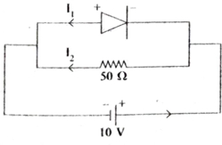
A
$0.0 \ A, 0.2 \ A$
B
$0.2 \ A, 0.0 \ A$
C
$10.0 \ A, 0.0 \ A$
D
$0.0 \ A, 0.0 \ A$
Solution
(A) In the given circuit,the diode is connected in reverse bias because the positive terminal of the battery is connected to the $n$-side (cathode) and the negative terminal is connected to the $p$-side (anode) of the diode.
Since the diode has infinite reverse bias resistance,the current $I_1$ flowing through the diode branch is $I_1 = 0.0 \ A$.
The resistor of $50 \ \Omega$ is connected in parallel to the battery of $10 \ V$. Therefore,the current $I_2$ flowing through the resistor is given by Ohm's law:
$I_2 = \frac{V}{R} = \frac{10 \ V}{50 \ \Omega} = 0.2 \ A$.
Thus,$I_1 = 0.0 \ A$ and $I_2 = 0.2 \ A$.
0 likes
View Solution346
EasyMCQ
When a forward bias is applied to a $p-n$ junction,it $\qquad$ .
A
raises the potential barrier.
B
lowers the potential barrier.
C
reduces the majority carrier to zero.
D
potential barrier remains same.
Solution
(B) When a $p-n$ junction is forward biased,the positive terminal of the external battery is connected to the $p$-side and the negative terminal to the $n$-side.
This external electric field opposes the internal electric field of the depletion region.
As a result,the width of the depletion layer decreases,and the potential barrier height is lowered.
Therefore,the correct option is $B$.
This external electric field opposes the internal electric field of the depletion region.
As a result,the width of the depletion layer decreases,and the potential barrier height is lowered.
Therefore,the correct option is $B$.
0 likes
View Solution347
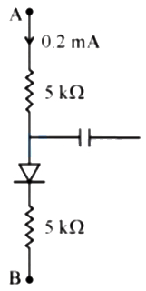
MediumMCQ
In the figure shown, if the diode forward voltage drop is $0.2 \, V$, the voltage difference between $A$ and $B$ is (in $V$)
A
$1.3$
B
$2.2$
C
$0$
D
$0.5$
Solution
(B) Given current $I = 0.2 \, mA = 0.2 \times 10^{-3} \, A$.
Voltage drop across the diode $V_d = 0.2 \, V$.
Resistors $R_1 = R_2 = 5 \, k\Omega = 5 \times 10^3 \, \Omega$.
The circuit consists of a resistor $R_1$, a diode, and a resistor $R_2$ in series.
The voltage drop across resistor $R_1$ is $V_{R1} = I \times R_1 = (0.2 \times 10^{-3} \, A) \times (5 \times 10^3 \, \Omega) = 1 \, V$.
The voltage drop across resistor $R_2$ is $V_{R2} = I \times R_2 = (0.2 \times 10^{-3} \, A) \times (5 \times 10^3 \, \Omega) = 1 \, V$.
The total voltage difference between $A$ and $B$ is the sum of the voltage drops across the components: $V_{AB} = V_{R1} + V_d + V_{R2} = 1 \, V + 0.2 \, V + 1 \, V = 2.2 \, V$.
0 likes
View Solution348
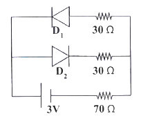
MediumMCQ
The circuit shown in the figure contains two ideal diodes $D_1$ and $D_2$. If a cell of emf $3 \text{ V}$ and negligible internal resistance is connected as shown,then the current through the $70 \Omega$ resistance (in ampere) is:
A
$0.01$
B
$0.02$
C
$0.03$
D
$0$
Solution
(C) In the given circuit,the positive terminal of the $3 \text{ V}$ battery is connected to the cathode of diode $D_1$ and the anode of diode $D_2$.
$1$. Diode $D_1$: The positive terminal of the battery is connected to the n-side (cathode) of $D_1$. Thus,$D_1$ is reverse-biased and acts as an open circuit (no current flows through this branch).
$2$. Diode $D_2$: The positive terminal of the battery is connected to the p-side (anode) of $D_2$. Thus,$D_2$ is forward-biased and acts as a closed switch (ideal diode has zero resistance).
$3$. Equivalent Resistance: Since $D_1$ is an open circuit,the current flows only through the branch containing $D_2$ and the $30 \Omega$ resistor,which is in series with the $70 \Omega$ resistor.
$R_{eq} = 30 \Omega + 70 \Omega = 100 \Omega$
$4$. Current Calculation: Using Ohm's law,$I = \frac{V}{R_{eq}}$
$I = \frac{3 \text{ V}}{100 \Omega} = 0.03 \text{ A}$
0 likes
View Solution349
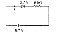
DifficultMCQ
$A$ $p-n$ junction diode is connected to a battery of emf $5.7 \ V$ in series with a resistor of $5 \ k\Omega$ such that it is forward biased. If the barrier potential of the diode is $0.7 \ V$,neglecting the diode resistance,the current in the circuit is:
A
$1.14 \ mA$
B
$1 \ mA$
C
$1 \ A$
D
$1.14 \ A$
Solution
(B) Given:
Battery emf,$V = 5.7 \ V$
Barrier potential of the diode,$V_B = 0.7 \ V$
Series resistance,$R_S = 5 \ k\Omega = 5 \times 10^3 \ \Omega$
In a forward-biased $p-n$ junction diode,the effective voltage across the resistor is the difference between the battery emf and the barrier potential.
Effective voltage,$V_{eff} = V - V_B = 5.7 \ V - 0.7 \ V = 5.0 \ V$
Using Ohm's law,the current $I$ in the circuit is:
$I = \frac{V_{eff}}{R_S} = \frac{5.0 \ V}{5 \times 10^3 \ \Omega} = 1 \times 10^{-3} \ A$
$I = 1 \ mA$
0 likes
View Solution350
EasyMCQ
When a $p-n$ junction diode is in forward bias,which type of charge carriers flows in the connecting wire?
A
Free electrons
B
Ions
C
Protons
D
Holes
Solution
(A) In a $p-n$ junction diode,the current in the semiconductor is due to both electrons and holes.
However,in the external connecting wires,the current is purely electronic.
When the diode is forward biased,the potential difference causes free electrons to flow through the external circuit (connecting wires) from the negative terminal to the positive terminal.
Therefore,the charge carriers flowing in the connecting wire are free electrons.
0 likes
View SolutionSemiconductor Electronics — PN Junction and Diode · Frequently Asked Questions
1Are these Semiconductor Electronics questions useful for JEE and NEET?
Yes. All questions in this section are mapped to JEE Main and NEET exam patterns. Previous year questions from JEE Main, NEET, GUJCET and state-level exams are included with full solutions.
2Can I switch to Hindi or Gujarati for these questions?
Yes. Use the language tabs in the hero section or the sidebar to view the same questions and solutions in English, Hindi or Gujarati.
3How do I generate a question paper from this subtopic?
Use the Vedclass Exam Paper Generator — select the chapter and subtopic, set difficulty, and generate Sets A, B, C, D automatically. First 3 chapters of every subject are free.
Vedclass Products
For Students
Vedclass Test Series
Mock tests in real JEE/NEET style with performance analysis. 5-day free trial.
Start Free TrialFor Teachers
Exam Paper Generator
Generate Set A/B/C/D papers from this chapter in 2 minutes. 3 chapters free.
Try FreeFor Institutes
Online Exam Module
Live online exams with unlimited students, 360° analytics & white-label branding.
See DemoFor Teachers & Institutes
Generate a Semiconductor Electronics Exam Paper in 2 Minutes
Select subtopic & difficulty — Sets A, B, C, D auto-generated with No Repeat logic.
First 3 chapters of every subject are free — no payment required.