
A English
Boolean Algebra and Logic Gates Questions in English
Class 12 Physics · Semiconductor Electronics · Boolean Algebra and Logic Gates
483+
Questions
English
Language
100%
With Solutions
Showing 46 of 483 questions in English
251
MediumMCQ
Which of the following gates is called a universal gate?
A
$NOT$ gate
B
$OR$ gate
C
$AND$ gate
D
$NAND$ gate
Solution
(D) universal gate is a logic gate that can be used to implement any other logic gate or Boolean function without the need for any other type of gate.
$NAND$ and $NOR$ gates are known as universal gates.
Since $NAND$ gate is listed among the options,it is the correct answer.
$NAND$ and $NOR$ gates are known as universal gates.
Since $NAND$ gate is listed among the options,it is the correct answer.
0 likes
View Solution252
DifficultMCQ
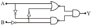
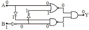
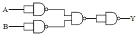
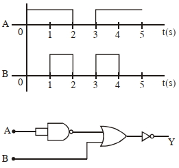
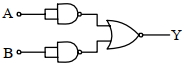
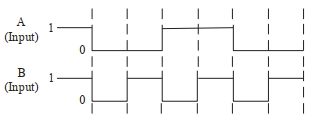
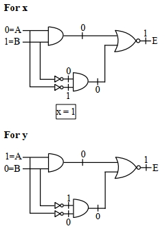
In the logic circuit shown in the figure,if inputs $A$ and $B$ are $0$ and $1$ respectively,the output at $Y$ is $x$. The value of $x$ is...........
A
$0$
B
$1$
C
$0$ or $1$
D
None of these
Solution
(A) Given inputs are $A = 0$ and $B = 1$.
$1$. The input $A=0$ goes to the $NOR$ gate and also to a $NOT$ gate. The output of this $NOT$ gate is $1$.
$2$. The input $B=1$ goes to a $NOT$ gate,so its output is $0$. This $0$ is fed to the $NAND$ gate and also to another $NOT$ gate,which outputs $1$.
$3$. The $NOR$ gate receives $A=0$ and the output of the second $NOT$ gate,which is $1$. Thus,the $NOR$ gate output is $\overline{0+1} = \overline{1} = 0$.
$4$. The $NAND$ gate receives the output of the first $NOT$ gate $(1)$ and the output of the $NOT$ gate connected to $B$ $(0)$. Thus,the $NAND$ gate output is $\overline{1 \cdot 0} = \overline{0} = 1$.
$5$. Finally,the $AND$ gate receives the outputs of the $NOR$ gate $(0)$ and the $NAND$ gate $(1)$. The output $Y$ is $0 \cdot 1 = 0$.
Therefore,$x = 0$.
0 likes
View Solution253
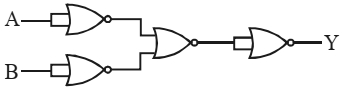
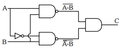
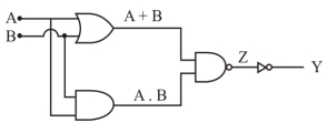
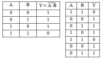
MediumMCQ
The output of the given combination of logic gates represents:
A
$AND$ Gate
B
$NAND$ Gate
C
$OR$ Gate
D
$NOR$ Gate
Solution
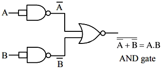
(B) $1$. The first two gates are $NOT$ gates (since inputs $A$ and $B$ are connected to both terminals of the $NOR$ gates). Thus,the outputs are $\bar{A}$ and $\bar{B}$.
$2$. These outputs are fed into a $NOR$ gate. The output of this gate is $\overline{\bar{A} + \bar{B}}$.
$3$. By De Morgan's theorem,$\overline{\bar{A} + \bar{B}} = \overline{\bar{A}} \cdot \overline{\bar{B}} = A \cdot B$.
$4$. This result $(A \cdot B)$ is then fed into a final $NOT$ gate (a $NOR$ gate with shorted inputs). The final output $Y$ is $\overline{A \cdot B}$.
$5$. The expression $\overline{A \cdot B}$ represents a $NAND$ gate.
0 likes
View Solution254
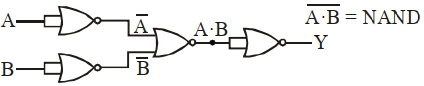
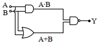
MediumMCQ
The following logic gate circuit is equivalent to which of the following gates?
A
$NOR$ Gate
B
$OR$ Gate
C
$AND$ Gate
D
$NAND$ Gate
Solution
(A) Let the inputs be $A$ and $B$. The first two $NAND$ gates act as $NOT$ gates because their inputs are shorted. Thus,the outputs of these gates are $\bar{A}$ and $\bar{B}$ respectively.
These are fed into a third $NAND$ gate,which produces the output $Y' = \overline{\bar{A} \cdot \bar{B}} = A + B$ (by De Morgan's Law).
This output $Y'$ is then fed into a final $NAND$ gate acting as a $NOT$ gate,resulting in the final output $Y = \overline{Y'} = \overline{A + B}$.
The Boolean expression $Y = \overline{A + B}$ corresponds to a $NOR$ gate.
Truth table:
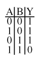
| $A$ | $B$ | $Y$ |
| $0$ | $0$ | $1$ |
| $0$ | $1$ | $0$ |
| $1$ | $0$ | $0$ |
| $1$ | $1$ | $0$ |
0 likes
View Solution255
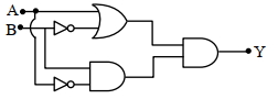
DifficultMCQ
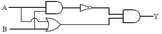
Which one of the following will be the output of the given circuit?
A
$NOR$ Gate
B
$NAND$ Gate
C
$AND$ Gate
D
$XOR$ Gate
Solution
(D) Let the inputs be $A$ and $B$.
$1$. The upper branch consists of an $AND$ gate followed by a $NOT$ gate,which is a $NAND$ gate. Its output is $\overline{A \cdot B}$.
$2$. The lower branch is an $OR$ gate. Its output is $(A + B)$.
$3$. These two outputs are fed into a final $AND$ gate.
$4$. The final output $Y = \overline{A \cdot B} \cdot (A + B)$.
$5$. Using Boolean algebra: $Y = (\overline{A} + \overline{B}) \cdot (A + B) = \overline{A}A + \overline{A}B + \overline{B}A + \overline{B}B$.
$6$. Since $\overline{A}A = 0$ and $\overline{B}B = 0$,we get $Y = \overline{A}B + A\overline{B}$.
$7$. This is the Boolean expression for an $XOR$ gate.
0 likes
View Solution256
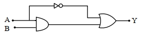
DifficultMCQ
The logic circuit shown above is equivalent to:
A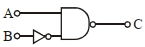
B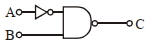
C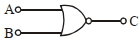
D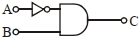
Solution
(B) The given circuit consists of an $OR$ gate where input $B$ is passed through a $NOT$ gate,and the output of the $OR$ gate is passed through another $NOT$ gate.
Let the inputs be $A$ and $B$. The input to the $OR$ gate becomes $A$ and $\bar{B}$.
The output of the $OR$ gate is $Y' = A + \bar{B}$.
The final output $C$ is the inversion of $Y'$,so $C = \overline{A + \bar{B}}$.
Using De Morgan's Law,$C = \bar{A} \cdot \overline{\bar{B}} = \bar{A} \cdot B$.
This expression $\bar{A} \cdot B$ represents an $AND$ gate with an inverted input $A$.
0 likes
View Solution257
DifficultMCQ
The truth table for the following logic circuit is ...... .
A
| $A, B, Y$ |
| $0, 0, 0$ |
| $0, 1, 1$ |
| $1, 0, 1$ |
| $1, 1, 0$ |
B
| $A, B, Y$ |
| $0, 0, 1$ |
| $0, 1, 0$ |
| $1, 0, 0$ |
| $1, 1, 1$ |
C
| $A, B, Y$ |
| $0, 0, 1$ |
| $0, 1, 0$ |
| $1, 0, 1$ |
| $1, 1, 0$ |
D
| $A, B, Y$ |
| $0, 0, 0$ |
| $0, 1, 1$ |
| $1, 0, 0$ |
| $1, 1, 1$ |
Solution
(B) The given circuit consists of two $AND$ gates,one $OR$ gate,and one $NOT$ gate (forming a $NOR$ gate at the output). The inputs to the first $AND$ gate are $A$ and $\bar{B}$. The inputs to the second $AND$ gate are $\bar{A}$ and $B$.
The output of the $OR$ gate is $(A \cdot \bar{B} + \bar{A} \cdot B)$.
The final output $Y$ is the inversion of this,so $Y = \overline{(A \cdot \bar{B} + \bar{A} \cdot B)}$.
Using De Morgan's theorem,$Y = \overline{(A \cdot \bar{B})} \cdot \overline{(\bar{A} \cdot B)} = (\bar{A} + B) \cdot (A + \bar{B})$.
Expanding this,$Y = \bar{A} \cdot A + \bar{A} \cdot \bar{B} + B \cdot A + B \cdot \bar{B} = 0 + \bar{A} \cdot \bar{B} + A \cdot B + 0 = A \cdot B + \bar{A} \cdot \bar{B}$.
This is the Boolean expression for an $XNOR$ gate.
| $A$ | $B$ | $Y$ |
| $0$ | $0$ | $1$ |
| $0$ | $1$ | $0$ |
| $1$ | $0$ | $0$ |
| $1$ | $1$ | $1$ |
0 likes
View Solution258
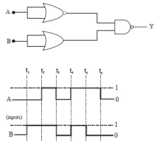
MediumMCQ
Draw the output signal $Y$ for the given combination of logic gates shown in the figure.
A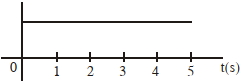
B
C
D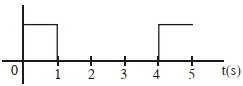
Solution
(D) The given circuit consists of a $NAND$ gate,an $OR$ gate,and a $NOT$ gate. Let the inputs be $A$ and $B$. The output of the $NAND$ gate is $\overline{A \cdot A} = \overline{A}$.
This output $\overline{A}$ and input $B$ are fed into an $OR$ gate,giving an intermediate output $Z = \overline{A} + B$.
Finally,this is passed through a $NOT$ gate to give the final output $Y = \overline{Z} = \overline{\overline{A} + B}$.
Using De Morgan's law,$\overline{\overline{A} + B} = \overline{\overline{A}} \cdot \overline{B} = A \cdot \overline{B}$.
Now,we analyze the truth table for $Y = A \cdot \overline{B}$:
- For $t = 0$ to $1$ s: $A=1, B=0 \implies Y = 1 \cdot \overline{0} = 1 \cdot 1 = 1$.
- For $t = 1$ to $2$ s: $A=1, B=1 \implies Y = 1 \cdot \overline{1} = 1 \cdot 0 = 0$.
- For $t = 2$ to $3$ s: $A=0, B=0 \implies Y = 0 \cdot \overline{0} = 0 \cdot 1 = 0$.
- For $t = 3$ to $4$ s: $A=1, B=1 \implies Y = 1 \cdot \overline{1} = 1 \cdot 0 = 0$.
- For $t = 4$ to $5$ s: $A=1, B=0 \implies Y = 1 \cdot \overline{0} = 1 \cdot 1 = 1$.
Thus,the output $Y$ is high $(1)$ from $t = 0$ to $1$ s and from $t = 4$ to $5$ s,and low $(0)$ otherwise. This matches the signal shown in option $D$.
0 likes
View Solution259
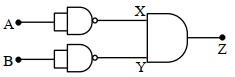
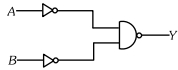
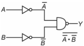
MediumMCQ
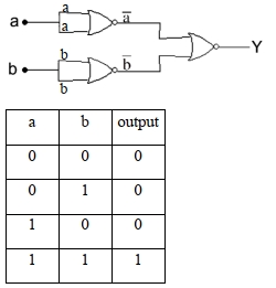
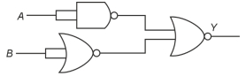
Identify the logic operation carried out by the given circuit :-
A
$OR$
B
$AND$
C
$NOR$
D
$NAND$
Solution
(C) The given circuit consists of two $NAND$ gates whose inputs are tied together,acting as $NOT$ gates,followed by an $AND$ gate.
Let the inputs be $A$ and $B$.
The outputs of the two $NOT$ gates are $X = \overline{A}$ and $Y = \overline{B}$.
The final output $Z$ is the $AND$ operation of $X$ and $Y$:
$Z = X \cdot Y = \overline{A} \cdot \overline{B}$.
Using De Morgan's theorem,$\overline{A} \cdot \overline{B} = \overline{A + B}$.
This is the Boolean expression for a $NOR$ gate.
Truth Table:
| $A, B$ | $X, Y$ | $Z$ |
|---|---|---|
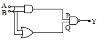
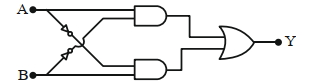
| $0, 0$ | $1, 1$ | $1$ |
| $0, 1$ | $1, 0$ | $0$ |
| $1, 0$ | $0, 1$ | $0$ |
| $1, 1$ | $0, 0$ | $0$ |
0 likes
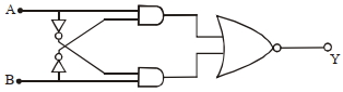
View Solution260
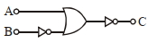
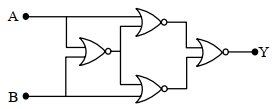
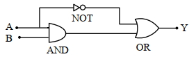
DifficultMCQ
Four $NOR$ gates are connected as shown in the figure. The truth table for the given figure is:
A
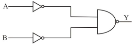
| $A, B$ | $Y$ |
| $0, 0$ | $1$ |
| $0, 1$ | $0$ |
| $1, 0$ | $1$ |
| $1, 1$ | $0$ |
B
| $A, B$ | $Y$ |
| $0, 0$ | $0$ |
| $0, 1$ | $1$ |
| $1, 0$ | $1$ |
| $1, 1$ | $0$ |
C
| $A, B$ | $Y$ |
| $0, 0$ | $0$ |
| $0, 1$ | $1$ |
| $1, 0$ | $0$ |
| $1, 1$ | $1$ |
D
| $A, B$ | $Y$ |
| $0, 0$ | $1$ |
| $0, 1$ | $0$ |
| $1, 0$ | $0$ |
| $1, 1$ | $1$ |
Solution
(B) Let the output of the first $NOR$ gate be $C = \overline{A+B}$.
This signal $C$ is fed into the next two $NOR$ gates along with inputs $A$ and $B$ respectively.
The outputs of these two gates are $D = \overline{A+C} = \overline{A+\overline{A+B}}$ and $E = \overline{B+C} = \overline{B+\overline{A+B}}$.
Using De Morgan's theorem,$D = \overline{A} \cdot (A+B) = \overline{A}A + \overline{A}B = 0 + \overline{A}B = \overline{A}B$.
Similarly,$E = \overline{B} \cdot (A+B) = \overline{B}A + \overline{B}B = A\overline{B} + 0 = A\overline{B}$.
The final output $Y$ is the $NOR$ of $D$ and $E$: $Y = \overline{D+E} = \overline{\overline{A}B + A\overline{B}}$.
This is the expression for an $XOR$ gate,which is $A \oplus B$.
The truth table for $A \oplus B$ is:
| $A, B$ | $Y$ |
| $0, 0$ | $0$ |
| $0, 1$ | $1$ |
| $1, 0$ | $1$ |
| $1, 1$ | $0$ |
0 likes
View Solution261
MediumMCQ
In the following logic circuit,the sequence of the inputs $A, B$ are $(0,0), (0,1), (1,0)$ and $(1,1)$. The output $Y$ for this sequence will be:
A
$1,1,1,0$
B
$0,1,0,1$
C
$1,0,1,0$
D
$0,0,1,1$
Solution
(A) The given circuit consists of an $AND$ gate,an $OR$ gate,and a $NAND$ gate.
The inputs to the $AND$ gate are $A$ and $B$,so its output is $A \cdot B$.
The inputs to the $OR$ gate are $A$ and $B$,so its output is $A + B$.
These two outputs are fed into a $NAND$ gate,so the final output $Y$ is given by:
$Y = \overline{(A \cdot B) \cdot (A + B)}$
Now,we calculate $Y$ for each input sequence $(A, B)$:
$1$. For $(0,0): Y = \overline{(0 \cdot 0) \cdot (0 + 0)} = \overline{0 \cdot 0} = \overline{0} = 1$
$2$. For $(0,1): Y = \overline{(0 \cdot 1) \cdot (0 + 1)} = \overline{0 \cdot 1} = \overline{0} = 1$
$3$. For $(1,0): Y = \overline{(1 \cdot 0) \cdot (1 + 0)} = \overline{0 \cdot 1} = \overline{0} = 1$
$4$. For $(1,1): Y = \overline{(1 \cdot 1) \cdot (1 + 1)} = \overline{1 \cdot 1} = \overline{1} = 0$
Thus,the sequence of outputs $Y$ is $1, 1, 1, 0$.
0 likes
View Solution262
DifficultMCQ
If ${V}_{A}$ and ${V}_{B}$ are the input voltages (either $5\, V$ or $0\, V$) and ${V}_{0}$ is the output voltage,then the two gates represented in the following circuit $(A)$ and $(B)$ are:
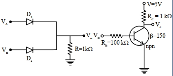
A
$AND$ and $OR$ Gate
B
$OR$ and $NOT$ Gate
C
$NAND$ and $NOR$ Gate
D
$AND$ and $NOT$ Gate
Solution
(B) For circuit $(A)$:
${V}_{A} = 5\, V \Rightarrow A = 1$,${V}_{A} = 0\, V \Rightarrow A = 0$
${V}_{B} = 5\, V \Rightarrow B = 1$,${V}_{B} = 0\, V \Rightarrow B = 0$
If $A = B = 0$,both diodes are reverse biased,so ${V}_{0} = 0\, V$.
If $A = 1, B = 0$,diode ${D}_{1}$ is forward biased,so ${V}_{0} = 5\, V$.
If $A = 0, B = 1$,diode ${D}_{2}$ is forward biased,so ${V}_{0} = 5\, V$.
If $A = 1, B = 1$,both diodes are forward biased,so ${V}_{0} = 5\, V$.
This truth table corresponds to an $OR$ gate.
For circuit $(B)$:
This is a common-emitter $npn$ transistor configuration.
When input voltage is $0\, V$ $(A = 0)$,the base-emitter junction is not forward biased,the transistor is in cut-off,and ${V}_{0} = 5\, V$ (logic $1$).
When input voltage is $5\, V$ $(A = 1)$,the base-emitter junction is forward biased,the transistor goes into saturation,and ${V}_{0} \approx 0\, V$ (logic $0$).
This inversion behavior corresponds to a $NOT$ gate.
Therefore,the gates are $OR$ and $NOT$.
0 likes
View Solution263
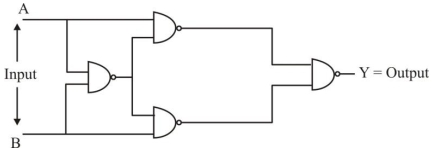
MediumMCQ
For the given circuit,the input digital signals are applied at the terminals $A, B$ and $C$. What would be the output at the terminal $y$?
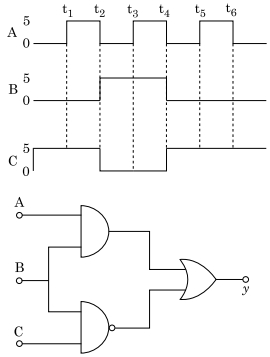
A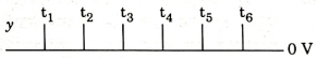
B
C
D
Solution
(D) The circuit consists of an $AND$ gate and a $NAND$ gate whose outputs are fed into an $OR$ gate. Let the inputs be $A, B, C$. The output of the $AND$ gate is $A \cdot B$. The output of the $NAND$ gate is $\overline{B \cdot C}$. The final output $Y$ of the $OR$ gate is $Y = (A \cdot B) + \overline{(B \cdot C)}$.
Analyzing the truth table for the intervals:
- Interval $0-t_1$: $A=0, B=0, C=1$. $Y = (0 \cdot 0) + \overline{(0 \cdot 1)} = 0 + 1 = 1$.
- Interval $t_1-t_2$: $A=1, B=0, C=1$. $Y = (1 \cdot 0) + \overline{(0 \cdot 1)} = 0 + 1 = 1$.
- Interval $t_2-t_3$: $A=0, B=1, C=0$. $Y = (0 \cdot 1) + \overline{(1 \cdot 0)} = 0 + 1 = 1$.
- Interval $t_3-t_4$: $A=1, B=1, C=0$. $Y = (1 \cdot 1) + \overline{(1 \cdot 0)} = 1 + 1 = 1$.
- Interval $t_4-t_5$: $A=0, B=0, C=1$. $Y = (0 \cdot 0) + \overline{(0 \cdot 1)} = 0 + 1 = 1$.
- Interval $t_5-t_6$: $A=1, B=0, C=1$. $Y = (1 \cdot 0) + \overline{(0 \cdot 1)} = 0 + 1 = 1$.
Since the output is $1$ $(5 \text{ V})$ for all intervals,the correct representation is a constant $5 \text{ V}$ signal.
0 likes
View Solution264
MediumMCQ
Identify the logic operation carried out by the given circuit.
A
$NAND$
B
$NOR$
C
$OR$
D
$AND$
Solution
(D) The given circuit consists of two $NAND$ gates acting as $NOT$ gates (since their inputs are shorted) followed by a $NOR$ gate.
Let the inputs be $A$ and $B$.
The output of the first $NAND$ gate (acting as $NOT$) is $\bar{A}$.
The output of the second $NAND$ gate (acting as $NOT$) is $\bar{B}$.
These two outputs are fed into a $NOR$ gate.
The output $Y$ of the $NOR$ gate is given by $Y = \overline{\bar{A} + \bar{B}}$.
Using De Morgan's theorem,$\overline{\bar{A} + \bar{B}} = \overline{\bar{A}} \cdot \overline{\bar{B}} = A \cdot B$.
Thus,the circuit performs the $AND$ operation.
0 likes
View Solution265
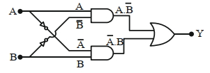
MediumMCQ
Find the truth table for the function $Y$ with inputs $A$ and $B$ represented in the following figure.
A
| $A$ | $B$ | $Y$ |
| $0$ | $0$ | $0$ |
| $0$ | $1$ | $1$ |
| $1$ | $0$ | $0$ |
| $1$ | $1$ | $1$ |
B
| $A$ | $B$ | $Y$ |
| $0$ | $0$ | $1$ |
| $0$ | $1$ | $0$ |
| $1$ | $0$ | $1$ |
| $1$ | $1$ | $1$ |
C
| $A$ | $B$ | $Y$ |
| $0$ | $0$ | $0$ |
| $0$ | $1$ | $0$ |
| $1$ | $0$ | $0$ |
| $1$ | $1$ | $1$ |
D
| $A$ | $B$ | $Y$ |
| $0$ | $0$ | $0$ |
| $0$ | $1$ | $1$ |
| $1$ | $0$ | $1$ |
| $1$ | $1$ | $1$ |
Solution
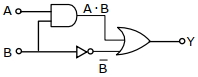
(B) The given circuit consists of an $AND$ gate,a $NOT$ gate,and an $OR$ gate.
The inputs to the $AND$ gate are $A$ and $B$,so its output is $A \cdot B$.
The input to the $NOT$ gate is $B$,so its output is $\bar{B}$.
These two outputs are then fed into an $OR$ gate,so the final output is $Y = A \cdot B + \bar{B}$.
Using Boolean algebra,$Y = A \cdot B + \bar{B} = (A + \bar{B}) \cdot (B + \bar{B}) = (A + \bar{B}) \cdot 1 = A + \bar{B}$.
Now,we construct the truth table:
| $A$ | $B$ | $A \cdot B$ | $\bar{B}$ | $Y = A \cdot B + \bar{B}$ |
| $0$ | $0$ | $0$ | $1$ | $1$ |
| $0$ | $1$ | $0$ | $0$ | $0$ |
| $1$ | $0$ | $0$ | $1$ | $1$ |
| $1$ | $1$ | $1$ | $0$ | $1$ |
0 likes
View Solution266
MediumMCQ
The truth table for the given logic circuit is:
A
| $A$ | $B$ | $C$ |
| $0$ | $0$ | $0$ |
| $0$ | $1$ | $0$ |
| $1$ | $0$ | $0$ |
| $1$ | $1$ | $1$ |
B
| $A$ | $B$ | $C$ |
| $0$ | $0$ | $1$ |
| $0$ | $1$ | $0$ |
| $1$ | $0$ | $1$ |
| $1$ | $1$ | $0$ |
C
| $A$ | $B$ | $C$ |
| $0$ | $0$ | $0$ |
| $0$ | $1$ | $0$ |
| $1$ | $0$ | $0$ |
| $1$ | $1$ | $1$ |
D
| $A$ | $B$ | $C$ |
| $0$ | $0$ | $0$ |
| $0$ | $1$ | $1$ |
| $1$ | $0$ | $1$ |
| $1$ | $1$ | $0$ |
Solution
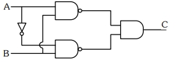
(B) The circuit consists of two $NAND$ gates whose outputs are fed into an $AND$ gate. Let the inputs be $A$ and $B$. The upper $NAND$ gate receives inputs $A$ and $B$,so its output is $\overline{A \cdot B}$. The lower $NAND$ gate receives inputs $\bar{A}$ (from the $NOT$ gate) and $B$,so its output is $\overline{\bar{A} \cdot B}$. The final output $C$ is the $AND$ operation of these two outputs: $C = (\overline{A \cdot B}) \cdot (\overline{\bar{A} \cdot B})$.
Using De Morgan's theorem,$\overline{A \cdot B} = \bar{A} + \bar{B}$ and $\overline{\bar{A} \cdot B} = A + \bar{B}$.
Thus,$C = (\bar{A} + \bar{B}) \cdot (A + \bar{B})$.
Using the distributive law,$C = \bar{A}A + \bar{A}\bar{B} + \bar{B}A + \bar{B}\bar{B}$.
Since $\bar{A}A = 0$ and $\bar{B}\bar{B} = \bar{B}$,we get $C = 0 + \bar{B}(\bar{A} + A) + \bar{B} = \bar{B}(1) + \bar{B} = \bar{B} + \bar{B} = \bar{B}$.
Therefore,the output $C$ is the $NOT$ of $B$ $(\bar{B})$.
| $A$ | $B$ | $C$ |
|---|---|---|
| $0$ | $0$ | $1$ |
| $0$ | $1$ | $0$ |
| $1$ | $0$ | $1$ |
| $1$ | $1$ | $0$ |
0 likes
View Solution267
MediumMCQ
Identify the logic operation performed by the given circuit.
A
$AND$ gate
B
$OR$ gate
C
$NOR$ gate
D
$NAND$ gate
Solution
(A) The circuit consists of two $NOR$ gates whose inputs are shorted,followed by a $NOR$ gate.
$1$. The first two gates are $NOR$ gates with inputs $A$ and $A$,and $B$ and $B$ respectively. Their outputs are $\overline{A+A} = \overline{A}$ and $\overline{B+B} = \overline{B}$.
$2$. These outputs are fed into a final $NOR$ gate.
$3$. The output $Y$ is given by $Y = \overline{\overline{A} + \overline{B}}$.
$4$. Using De Morgan's Law,$\overline{\overline{A} + \overline{B}} = \overline{\overline{A}} \cdot \overline{\overline{B}} = A \cdot B$.
$5$. The expression $Y = A \cdot B$ represents an $AND$ gate.
0 likes
View Solution268
MediumMCQ
Identify the correct Logic Gate for the following output $(Y)$ of two inputs $A$ and $B$.
A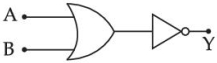
B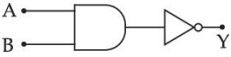
C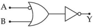
D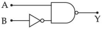
Solution
(A) To identify the logic gate,we analyze the truth table from the given timing diagram:
From the truth table,we observe that the output $Y$ is $1$ if either $A$ or $B$ (or both) is $1$. This is the characteristic behavior of an $OR$ gate. The expression for an $OR$ gate is $Y = A + B$.
| $A$ | $B$ | $Y$ |
|---|---|---|
| $0$ | $0$ | $0$ |
| $0$ | $1$ | $1$ |
| $1$ | $0$ | $1$ |
| $1$ | $1$ | $1$ |
From the truth table,we observe that the output $Y$ is $1$ if either $A$ or $B$ (or both) is $1$. This is the characteristic behavior of an $OR$ gate. The expression for an $OR$ gate is $Y = A + B$.
0 likes
View Solution269
DifficultMCQ
In the following circuit,the correct relation between output $(Y)$ and inputs $A$ and $B$ will be
A
$Y = AB$
B
$Y = A + B$
C
$Y = \overline{AB}$
D
$Y = \overline{A + B}$
Solution
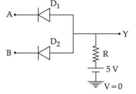
(C) The circuit consists of two diodes $D_1$ and $D_2$ connected to inputs $A$ and $B$,followed by an $npn$ transistor.
If both inputs $A$ and $B$ are at low potential $(0)$,the diodes are forward biased,and the potential at point $X$ is low. The transistor remains in the cut-off state,so the output $Y$ is at high potential $(1)$.
If either $A$ or $B$ is at high potential $(1)$,the corresponding diode is reverse biased,but the other diode or the resistor path keeps the potential at $X$ low enough such that the transistor remains off,resulting in $Y = 1$.
If both $A$ and $B$ are at high potential $(1)$,the potential at $X$ becomes high enough to turn the transistor $ON$. When the transistor is $ON$,the collector-emitter path acts as a short circuit to ground,pulling the output $Y$ to low potential $(0)$.
This behavior corresponds to the $NAND$ gate logic,where $Y = \overline{AB}$.
0 likes
View Solution270
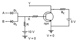
DifficultMCQ
In the circuit,the logical value of $A = 1$ or $B = 1$ when the potential at $A$ or $B$ is $5 \, V$,and the logical value of $A = 0$ or $B = 0$ when the potential at $A$ or $B$ is $0 \, V$. The truth table of the given circuit will be:
A
| $A$ | $B$ | $Y$ |
| $0$ | $0$ | $0$ |
| $1$ | $0$ | $0$ |
| $0$ | $1$ | $0$ |
| $1$ | $1$ | $1$ |
B
| $A$ | $B$ | $Y$ |
| $0$ | $0$ | $0$ |
| $1$ | $0$ | $1$ |
| $0$ | $1$ | $1$ |
| $1$ | $1$ | $1$ |
C
| $A$ | $B$ | $Y$ |
| $0$ | $0$ | $0$ |
| $1$ | $0$ | $0$ |
| $0$ | $1$ | $0$ |
| $1$ | $1$ | $0$ |
D
| $A$ | $B$ | $Y$ |
| $0$ | $0$ | $1$ |
| $1$ | $0$ | $1$ |
| $0$ | $1$ | $1$ |
| $1$ | $1$ | $0$ |
Solution
(A) In the given circuit,if either input $A$ or $B$ is at $0 \, V$ (logical $0$),the corresponding diode ($D_1$ or $D_2$) becomes forward-biased. This pulls the output potential $Y$ down to approximately $0 \, V$ (logical $0$).
If both inputs $A$ and $B$ are at $5 \, V$ (logical $1$),both diodes are reverse-biased. No current flows through the diodes,and the output $Y$ is pulled up to $5 \, V$ (logical $1$) through the resistor $R$.
This behavior corresponds to an $AND$ gate,where the output is $1$ only if both inputs are $1$. The truth table is:
| $A$ | $B$ | $Y$ |
| $0$ | $0$ | $0$ |
| $0$ | $1$ | $0$ |
| $1$ | $0$ | $0$ |
| $1$ | $1$ | $1$ |
0 likes
View Solution271
MediumMCQ
$A$ logic gate circuit has two inputs $A$ and $B$ and output $Y$. The voltage waveforms of $A, B$ and $Y$ are shown below. Identify the logic gate circuit.
A
$AND$ gate
B
$OR$ gate
C
$NOR$ gate
D
$NAND$ gate
Solution
(A) By analyzing the given voltage waveforms,we can construct the truth table for the inputs $A, B$ and output $Y$:
Comparing this truth table with the standard logic gates:
- For an $AND$ gate,the output is $1$ only when both inputs are $1$.
- The observed truth table matches the behavior of an $AND$ gate exactly.
Therefore,the logic gate is an $AND$ gate.
| $A$ | $B$ | $Y$ |
| $0$ | $0$ | $0$ |
| $0$ | $1$ | $0$ |
| $1$ | $0$ | $0$ |
| $1$ | $1$ | $1$ |
Comparing this truth table with the standard logic gates:
- For an $AND$ gate,the output is $1$ only when both inputs are $1$.
- The observed truth table matches the behavior of an $AND$ gate exactly.
Therefore,the logic gate is an $AND$ gate.
0 likes
View Solution272
MediumMCQ
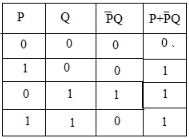
The Boolean expression $P + \overline{P}Q$,where $P$ and $Q$ are the inputs of the logic circuit,represents
A
$AND$ gate
B
$NAND$ gate
C
$NOT$ gate
D
$OR$ gate
Solution
(D) Using the distributive law of Boolean algebra,the expression can be simplified as follows:
$P + \overline{P}Q = (P + \overline{P}) \cdot (P + Q)$
Since $(P + \overline{P}) = 1$,the expression becomes:
$1 \cdot (P + Q) = P + Q$
The expression $P + Q$ represents the output of an $OR$ gate.
Alternatively,we can construct the truth table:
The output column for $P + \overline{P}Q$ matches the truth table of an $OR$ gate. Thus,the correct option is $D$.
$P + \overline{P}Q = (P + \overline{P}) \cdot (P + Q)$
Since $(P + \overline{P}) = 1$,the expression becomes:
$1 \cdot (P + Q) = P + Q$
The expression $P + Q$ represents the output of an $OR$ gate.
Alternatively,we can construct the truth table:
| $P$ | $Q$ | $\overline{P}$ | $\overline{P}Q$ | $P + \overline{P}Q$ |
|---|---|---|---|---|
| $0$ | $0$ | $1$ | $0$ | $0$ |
| $1$ | $0$ | $0$ | $0$ | $1$ |
| $0$ | $1$ | $1$ | $1$ | $1$ |
| $1$ | $1$ | $0$ | $0$ | $1$ |
The output column for $P + \overline{P}Q$ matches the truth table of an $OR$ gate. Thus,the correct option is $D$.
0 likes
View Solution273
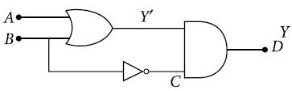
MediumMCQ
The output $D$ for the given circuit is:
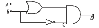
A
$(A + B) \cdot \overline{B}$
B
$(A \cdot B) \cdot \overline{B}$
C
$(A + B) \cdot B$
D
$(A \cdot B) \cdot B$
Solution
(A) $1$. The circuit consists of an $OR$ gate,a $NOT$ gate,and an $AND$ gate.
$2$. The inputs to the $OR$ gate are $A$ and $B$,so its output is $Y' = A + B$.
$3$. The input $B$ is also passed through a $NOT$ gate,so its output is $\overline{B}$.
$4$. The $AND$ gate takes $Y'$ and $\overline{B}$ as inputs.
$5$. Therefore,the final output $D$ is $D = Y' \cdot \overline{B} = (A + B) \cdot \overline{B}$.
0 likes
View Solution274
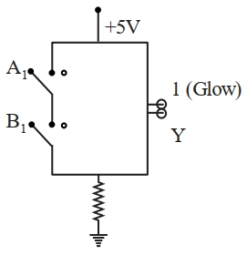
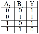
MediumMCQ
The logic gate equivalent to the given circuit diagram is:
A
$OR$
B
$NAND$
C
$NOR$
D
$AND$
Solution
(B) In the given circuit,the switches $A_1$ and $B_1$ are connected in parallel. The output $Y$ is taken across the resistor connected to the ground.
When both switches $A_1$ and $B_1$ are open (logic $0$),the output $Y$ is connected to $+5 \text{V}$ (logic $1$).
When either $A_1$ or $B_1$ is closed (logic $1$),the output $Y$ remains connected to $+5 \text{V}$ (logic $1$).
When both switches $A_1$ and $B_1$ are closed (logic $1$),the circuit is shorted to ground,and the output $Y$ becomes $0 \text{V}$ (logic $0$).
The truth table is:
| $A_1$ | $B_1$ | $Y$ |
|---|---|---|
| $0$ | $0$ | $1$ |
| $0$ | $1$ | $1$ |
| $1$ | $0$ | $1$ |
| $1$ | $1$ | $0$ |
This truth table corresponds to the $NAND$ gate,where $Y = \overline{A_1 \cdot B_1}$.
0 likes
View Solution275
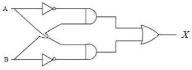
MediumMCQ
For the given logic gates combination,the correct truth table will be
A
B
C
D
Solution
(C) The given circuit consists of two $NOT$ gates,two $AND$ gates,and one $OR$ gate. Let the inputs be $A$ and $B$.
$1$. The top $AND$ gate receives inputs $\bar{A}$ and $B$. Its output is $Y_1 = \bar{A} \cdot B$.
$2$. The bottom $AND$ gate receives inputs $A$ and $\bar{B}$. Its output is $Y_2 = A \cdot \bar{B}$.
$3$. The final $OR$ gate combines these outputs: $X = Y_1 + Y_2 = \bar{A}B + A\bar{B}$.
This is the Boolean expression for an $XOR$ gate.
The truth table for an $XOR$ gate is:
- If $A=0, B=0$,then $X = 0 \cdot 0 + 0 \cdot 1 = 0$.
- If $A=0, B=1$,then $X = 1 \cdot 1 + 0 \cdot 0 = 1$.
- If $A=1, B=0$,then $X = 0 \cdot 0 + 1 \cdot 1 = 1$.
- If $A=1, B=1$,then $X = 0 \cdot 1 + 1 \cdot 0 = 0$.
Thus,the correct truth table is the one where $X=1$ only when $A$ and $B$ are different,which corresponds to option $C$.
0 likes
View Solution276
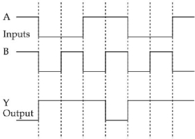
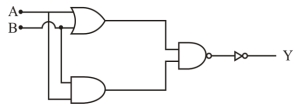
MediumMCQ
The output waveform of the given logical circuit for the following inputs $A$ and $B$ as shown below,is:
A
B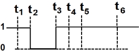
C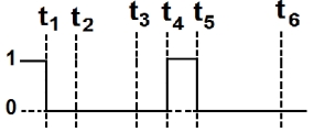
D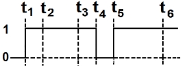
Solution
(D) The circuit consists of two $NAND$ gates as $NOT$ gates (since both inputs are tied together) followed by a $NAND$ gate.
$1$. The first $NAND$ gate with inputs $A$ and $A$ gives output $Y_1 = \overline{A \cdot A} = \overline{A}$.
$2$. The second $NAND$ gate with inputs $B$ and $B$ gives output $Y_2 = \overline{B \cdot B} = \overline{B}$.
$3$. The final $NAND$ gate takes $Y_1$ and $Y_2$ as inputs,so the final output $Y = \overline{Y_1 \cdot Y_2} = \overline{\overline{A} \cdot \overline{B}}$.
$4$. Using De Morgan's theorem,$\overline{\overline{A} \cdot \overline{B}} = \overline{\overline{A}} + \overline{\overline{B}} = A + B$.
$5$. Thus,the circuit acts as an $OR$ gate.
$6$. Analyzing the input waveforms:
- For $t < t_1$: $A=0, B=0 \implies Y = 0+0 = 0$.
- For $t_1 < t < t_2$: $A=1, B=0 \implies Y = 1+0 = 1$.
- For $t_2 < t < t_3$: $A=1, B=1 \implies Y = 1+1 = 1$.
- For $t_3 < t < t_4$: $A=0, B=1 \implies Y = 0+1 = 1$.
- For $t_4 < t < t_5$: $A=0, B=0 \implies Y = 0+0 = 0$.
- For $t_5 < t < t_6$: $A=1, B=0 \implies Y = 1+0 = 1$.
- For $t > t_6$: $A=0, B=0 \implies Y = 0+0 = 0$.
Comparing this with the given options,the waveform matches option $D$.
0 likes
View Solution277
MediumMCQ
The output $Y$ for the inputs $A$ and $B$ of the circuit is given by the truth table of the shown circuit:
A
| $A$ | $B$ | $Y$ |
|---|---|---|
| $0$ | $0$ | $1$ |
| $0$ | $1$ | $1$ |
| $1$ | $0$ | $1$ |
| $1$ | $1$ | $0$ |
B
| $A$ | $B$ | $Y$ |
|---|---|---|
| $0$ | $0$ | $1$ |
| $0$ | $1$ | $0$ |
| $1$ | $0$ | $0$ |
| $1$ | $1$ | $1$ |
C
| $A$ | $B$ | $Y$ |
|---|---|---|
| $0$ | $0$ | $0$ |
| $0$ | $1$ | $1$ |
| $1$ | $0$ | $1$ |
| $1$ | $1$ | $1$ |
D
| $A$ | $B$ | $Y$ |
|---|---|---|
| $0$ | $0$ | $0$ |
| $0$ | $1$ | $1$ |
| $1$ | $0$ | $1$ |
| $1$ | $1$ | $0$ |
Solution
(D) The given circuit consists of four $NAND$ gates. Let the inputs be $A$ and $B$.
$1$. The first $NAND$ gate (top) has inputs $A$ and the output of the middle $NAND$ gate (which acts as a $NOT$ gate for $A$ and $B$ combined, but here it is a $NAND$ gate with inputs $A$ and $B$). Let the middle gate output be $C = \overline{A \cdot B}$.
$2$. The top $NAND$ gate has inputs $A$ and $C$. Its output is $Y_1 = \overline{A \cdot C} = \overline{A \cdot (\overline{A \cdot B})} = \overline{A \cdot (\overline{A} + \overline{B})} = \overline{A \cdot \overline{A} + A \cdot \overline{B}} = \overline{0 + A \cdot \overline{B}} = \overline{A \cdot \overline{B}} = \overline{A} + B$.
$3$. Similarly, the bottom $NAND$ gate has inputs $B$ and $C$. Its output is $Y_2 = \overline{B \cdot C} = \overline{B \cdot (\overline{A \cdot B})} = \overline{B \cdot (\overline{A} + \overline{B})} = \overline{B \cdot \overline{A} + B \cdot \overline{B}} = \overline{B \cdot \overline{A} + 0} = \overline{B \cdot \overline{A}} = \overline{B} + A$.
$4$. The final $NAND$ gate has inputs $Y_1$ and $Y_2$. Its output is $Y = \overline{Y_1 \cdot Y_2} = \overline{(\overline{A} + B) \cdot (\overline{B} + A)} = \overline{\overline{A} \cdot \overline{B} + \overline{A} \cdot A + B \cdot \overline{B} + B \cdot A} = \overline{\overline{A} \cdot \overline{B} + 0 + 0 + A \cdot B} = \overline{\overline{A} \cdot \overline{B}} \cdot \overline{A \cdot B} = (A + B) \cdot (\overline{A} + \overline{B}) = A \cdot \overline{A} + A \cdot \overline{B} + B \cdot \overline{A} + B \cdot \overline{B} = 0 + A \cdot \overline{B} + \overline{A} \cdot B + 0 = A \oplus B$.
Thus, the circuit represents an $XOR$ gate. The truth table for $XOR$ is given in option $D$.
0 likes
View Solution278
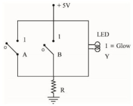
MediumMCQ
Identify the equivalent logic gate represented by the given circuit.
A
$OR$
B
$NOR$
C
$AND$
D
$NAND$
Solution
(A) In the given circuit,two switches are connected in parallel with the $LED$. The $LED$ glows when current flows through it,which happens when at least one of the switches is closed $(1)$. If both switches are open $(0)$,the circuit is incomplete and the $LED$ does not glow $(0)$.
This truth table corresponds to the $OR$ gate.
| $A$ | $B$ | $LED$ |
| $0$ | $0$ | $0$ |
| $0$ | $1$ | $1$ |
| $1$ | $0$ | $1$ |
| $1$ | $1$ | $1$ |
This truth table corresponds to the $OR$ gate.
0 likes
View Solution279
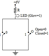
MediumMCQ
Name the logic gate equivalent to the diagram attached.
A
$OR$
B
$NOR$
C
$NAND$
D
$AND$
Solution
(B) In the given circuit,the switches $A$ and $B$ are connected in parallel to the ground through a resistor $R$. The output $Y$ is taken across the resistor $R$.
When both switches $A$ and $B$ are open (logic $0$),the current from the $+5 \text{V}$ source flows through the resistor $R$,causing the $LED$ to glow (logic $1$).
When either switch $A$ or switch $B$ (or both) is closed (logic $1$),the current is bypassed directly to the ground,and no current flows through the resistor $R$,so the $LED$ does not glow (logic $0$).
The truth table is:
$A=0, B=0 \Rightarrow Y=1$
$A=0, B=1 \Rightarrow Y=0$
$A=1, B=0 \Rightarrow Y=0$
$A=1, B=1 \Rightarrow Y=0$
This truth table corresponds to the $NOR$ gate.
0 likes
View Solution280
MediumMCQ
For the logic circuit shown,the output waveform at $Y$ is
A
B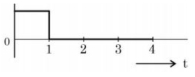
C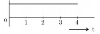
D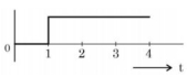
Solution
(D) The given circuit consists of two $NAND$ gates at the input followed by another $NAND$ gate. Let the inputs be $A$ and $B$. The output of the first two $NAND$ gates are $\overline{A}$ and $\overline{B}$ respectively (since they act as $NOT$ gates). The final $NAND$ gate takes $\overline{A}$ and $\overline{B}$ as inputs. The output $Y$ is given by $Y = \overline{\overline{A} \cdot \overline{B}}$. By De Morgan's theorem,$Y = \overline{\overline{A}} + \overline{\overline{B}} = A + B$. Thus,the circuit acts as an $OR$ gate.
Analyzing the waveforms:
For $t=0$ to $1$: $A=0, B=0 \implies Y = 0+0 = 0$.
For $t=1$ to $2$: $A=0, B=1 \implies Y = 0+1 = 1$.
For $t=2$ to $3$: $A=1, B=0 \implies Y = 1+0 = 1$.
For $t=3$ to $4$: $A=1, B=1 \implies Y = 1+1 = 1$.
Thus,the output $Y$ is $0$ from $t=0$ to $1$ and $1$ from $t=1$ to $4$.
0 likes
View Solution281
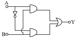
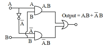
MediumMCQ
The logic performed by the circuit shown in the figure is equivalent to:
A
$AND$
B
$NAND$
C
$OR$
D
$NOR$
Solution
(A) The circuit consists of two $NOR$ gates used as $NOT$ gates at the input,followed by a $NOR$ gate at the output.
Input $a$ is fed into a $NOR$ gate with both inputs tied together,resulting in output $\bar{a}$.
Input $b$ is fed into a $NOR$ gate with both inputs tied together,resulting in output $\bar{b}$.
These outputs $\bar{a}$ and $\bar{b}$ are then fed into a final $NOR$ gate.
The final output $Y$ is given by $Y = \overline{\bar{a} + \bar{b}}$.
Using De Morgan's theorem,$\overline{\bar{a} + \bar{b}} = \overline{\bar{a}} \cdot \overline{\bar{b}} = a \cdot b$.
This is the Boolean expression for an $AND$ gate.
Thus,the circuit is equivalent to an $AND$ gate.
0 likes
View Solution282
MediumMCQ
The logic operations performed by the given digital circuit is equivalent to:
A
$AND$
B
$NOR$
C
$OR$
D
$NAND$
Solution
(A) The inputs to the circuit are $A$ and $B$.
The output of the $OR$ gate is $(A+B)$.
The output of the $AND$ gate is $(A \cdot B)$.
These two outputs are fed into a $NAND$ gate,which produces an output $Z = \overline{(A+B) \cdot (A \cdot B)}$.
This output $Z$ is then passed through a $NOT$ gate,resulting in the final output $Y = \bar{Z} = \overline{\overline{(A+B) \cdot (A \cdot B)}} = (A+B) \cdot (A \cdot B)$.
Using the distributive law of Boolean algebra,$(A+B) \cdot (A \cdot B) = (A \cdot A \cdot B) + (B \cdot A \cdot B) = (A \cdot B) + (A \cdot B) = A \cdot B$.
Thus,$Y = A \cdot B$,which is the Boolean expression for an $AND$ gate.
0 likes
View Solution283
MediumMCQ
For the following circuit and given inputs $A$ and $B$, choose the correct option for output $Y$.
A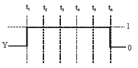
B
C
D
Solution
(B) The circuit consists of two $OR$ gates followed by a $NAND$ gate. Let the outputs of the two $OR$ gates be $Y_1$ and $Y_2$. Then $Y_1 = A + B$ and $Y_2 = A + B$. However, looking closely at the diagram, the top gate is a $NOR$ gate and the bottom is an $OR$ gate. Let's re-evaluate: The top gate is a $NOR$ gate, so its output is $Y_1 = \overline{A+B}$. The bottom gate is an $OR$ gate, so its output is $Y_2 = B+B = B$. The final gate is a $NAND$ gate, so the output $Y = \overline{Y_1 \cdot Y_2} = \overline{\overline{(A+B)} \cdot B} = (A+B) + \bar{B} = A + B + \bar{B} = A + 1 = 1$. Thus, the output $Y$ is always $1$ regardless of the inputs $A$ and $B$.
0 likes
View Solution284
MediumMCQ
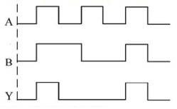
The output from a $NAND$ gate having inputs $A$ and $B$ given below will be:
A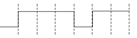
B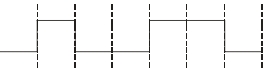
C
D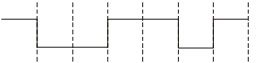
Solution
(D) $NAND$ gate produces a low output $(0)$ only when both inputs are high $(1)$. Otherwise, it produces a high output $(1)$. The truth table for a $NAND$ gate is:
| $A$ | $B$ | $Y = \overline{A \cdot B}$ |
|---|---|---|
| $0$ | $0$ | $1$ |
| $0$ | $1$ | $1$ |
| $1$ | $0$ | $1$ |
| $1$ | $1$ | $0$ |
By analyzing the input waveforms for $A$ and $B$ at different time intervals:
$1$. For the first interval, $A=1, B=1$, so $Y=0$.
$2$. For the second interval, $A=0, B=0$, so $Y=1$.
$3$. For the third interval, $A=0, B=1$, so $Y=1$.
$4$. For the fourth interval, $A=1, B=0$, so $Y=1$.
$5$. For the fifth interval, $A=1, B=1$, so $Y=0$.
$6$. For the sixth interval, $A=0, B=0$, so $Y=1$.
$7$. For the seventh interval, $A=0, B=1$, so $Y=1$.
Comparing this sequence $(0, 1, 1, 1, 0, 1, 1)$ with the given options, the waveform in image $D$ matches this output.
0 likes
View Solution285
MediumMCQ
For the following logic circuit,the truth table is:
A
| $A$ | $B$ | $Y$ |
| $0$ | $0$ | $0$ |
| $0$ | $1$ | $0$ |
| $1$ | $0$ | $0$ |
| $1$ | $1$ | $1$ |
B
| $A$ | $B$ | $Y$ |
| $0$ | $0$ | $1$ |
| $0$ | $1$ | $1$ |
| $1$ | $0$ | $1$ |
| $1$ | $1$ | $0$ |
C
| $A$ | $B$ | $Y$ |
| $0$ | $0$ | $0$ |
| $0$ | $1$ | $1$ |
| $1$ | $0$ | $1$ |
| $1$ | $1$ | $1$ |
D
| $A$ | $B$ | $Y$ |
| $0$ | $0$ | $1$ |
| $0$ | $1$ | $0$ |
| $1$ | $0$ | $1$ |
| $1$ | $1$ | $0$ |
Solution
(C) The given circuit consists of two $NOT$ gates followed by a $NAND$ gate.
Let the inputs be $A$ and $B$.
The outputs of the $NOT$ gates are $\bar{A}$ and $\bar{B}$.
These are the inputs to the $NAND$ gate.
Therefore,the output $Y = \overline{\bar{A} \cdot \bar{B}}$.
Using De Morgan's theorem,$\overline{\bar{A} \cdot \bar{B}} = \overline{\bar{A}} + \overline{\bar{B}} = A + B$.
This is the Boolean expression for an $OR$ gate.
The truth table for an $OR$ gate is:
| $A$ | $B$ | $Y$ |
| $0$ | $0$ | $0$ |
| $0$ and $1$ | $1$ | $1$ |
| $1$ and $0$ | $0$ | $1$ |
| $1$ and $1$ | $1$ | $1$ |
0 likes
View Solution286
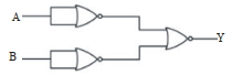
DifficultMCQ
The truth table of the given circuit diagram is:
A
| $A$ | $B$ | $y$ |
| $0$ | $0$ | $1$ |
| $0$ | $1$ | $0$ |
| $1$ | $0$ | $0$ |
| $1$ | $1$ | $1$ |
B
| $A$ | $B$ | $y$ |
| $0$ | $0$ | $0$ |
| $0$ | $1$ | $1$ |
| $1$ | $0$ | $1$ |
| $1$ | $1$ | $0$ |
C
| $A$ | $B$ | $y$ |
| $0$ | $0$ | $0$ |
| $0$ | $1$ | $0$ |
| $1$ | $0$ | $0$ |
| $1$ | $1$ | $1$ |
D
| $A$ | $B$ | $y$ |
| $0$ | $0$ | $1$ |
| $0$ | $1$ | $1$ |
| $1$ | $0$ | $1$ |
| $1$ | $1$ | $0$ |
Solution
(B) The circuit consists of two $AND$ gates,two $NOT$ gates,and one $OR$ gate.
The inputs to the first $AND$ gate are $A$ and $\overline{B}$,so its output is $A \cdot \overline{B}$.
The inputs to the second $AND$ gate are $\overline{A}$ and $B$,so its output is $\overline{A} \cdot B$.
The final $OR$ gate combines these outputs to give $Y = A \cdot \overline{B} + \overline{A} \cdot B$.
This is the Boolean expression for an $XOR$ gate.
The truth table for an $XOR$ gate is:
- If $A=0, B=0$,then $Y=0$.
- If $A=0, B=1$,then $Y=1$.
- If $A=1, B=0$,then $Y=1$.
- If $A=1, B=1$,then $Y=0$.
Comparing this with the given options,option $B$ is correct.
0 likes
View Solution287
DifficultMCQ
The truth table for this given circuit is:
A
| $A$ | $B$ | $Y$ |
|---|---|---|
| $0$ | $0$ | $1$ |
| $0$ | $1$ | $1$ |
| $1$ | $0$ | $1$ |
| $1$ | $1$ | $0$ |
B
| $A$ | $B$ | $Y$ |
|---|---|---|
| $0$ | $0$ | $0$ |
| $0$ | $1$ | $1$ |
| $1$ | $0$ | $0$ |
| $1$ | $1$ | $1$ |
C
| $A$ | $B$ | $Y$ |
|---|---|---|
| $0$ | $0$ | $0$ |
| $0$ | $1$ | $0$ |
| $1$ | $0$ | $0$ |
| $1$ | $1$ | $1$ |
D
| $A$ | $B$ | $Y$ |
|---|---|---|
| $0$ | $0$ | $0$ |
| $0$ | $1$ | $1$ |
| $1$ | $0$ | $1$ |
| $1$ | $1$ | $0$ |
Solution
(B) The given circuit consists of two $AND$ gates and one $OR$ gate. The inputs to the first $AND$ gate are $A$ and $B$,so its output is $A \cdot B$.
The input $A$ passes through a $NOT$ gate,becoming $\overline{A}$. This $\overline{A}$ and input $B$ are fed into the second $AND$ gate,so its output is $\overline{A} \cdot B$.
These two outputs are then fed into an $OR$ gate,giving the final output $Y = (A \cdot B) + (\overline{A} \cdot B)$.
Using Boolean algebra: $Y = (A + \overline{A}) \cdot B$.
Since $A + \overline{A} = 1$,we get $Y = 1 \cdot B = B$.
Thus,the output $Y$ is equal to input $B$. Checking the truth table for $Y = B$:
If $A=0, B=0$,then $Y=0$.
If $A=0, B=1$,then $Y=1$.
If $A=1, B=0$,then $Y=0$.
If $A=1, B=1$,then $Y=1$.
This matches option $B$.
0 likes
View Solution288
DifficultMCQ
Identify the logic operation performed by the given circuit.
A
$NAND$
B
$NOR$
C
$OR$
D
$AND$
Solution
(C) The circuit consists of two $NOT$ gates connected to the inputs $A$ and $B$,followed by a $NAND$ gate.
$1$. The inputs to the $NAND$ gate are $\overline{A}$ and $\overline{B}$.
$2$. The output $Y$ of the $NAND$ gate is given by $Y = \overline{\overline{A} \cdot \overline{B}}$.
$3$. According to De Morgan's law,$\overline{X \cdot Y} = \overline{X} + \overline{Y}$.
$4$. Applying this to our expression: $Y = \overline{\overline{A}} + \overline{\overline{B}} = A + B$.
$5$. The expression $Y = A + B$ represents the $OR$ logic operation.
0 likes
View Solution289
DifficultMCQ
The output of the given circuit diagram is
A
| $A, B, Y$ |
| $0, 0, 0$ |
| $1, 0, 0$ |
| $0, 1, 0$ |
| $1, 1, 1$ |
B
| $A, B, Y$ |
| $0, 0, 0$ |
| $1, 0, 1$ |
| $0, 1, 1$ |
| $1, 1, 0$ |
C
| $A, B, Y$ |
| $0, 0, 0$ |
| $1, 0, 0$ |
| $0, 1, 0$ |
| $1, 1, 0$ |
D
| $A, B, Y$ |
| $0, 0, 0$ |
| $1, 0, 0$ |
| $0, 1, 1$ |
| $1, 1, 0$ |
Solution
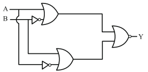
(C) The circuit consists of two $OR$ gates whose inputs are modified by $NOT$ gates,and their outputs are fed into a $NOR$ gate.
Let the inputs be $A$ and $B$.
The upper $OR$ gate has inputs $A$ and $\overline{B}$,so its output is $Y_1 = A + \overline{B}$.
The lower $OR$ gate has inputs $B$ and $\overline{A}$,so its output is $Y_2 = \overline{A} + B$.
These outputs $Y_1$ and $Y_2$ are fed into a $NOR$ gate,so the final output is $Y = \overline{Y_1 + Y_2} = \overline{(A + \overline{B}) + (\overline{A} + B)}$.
Let's construct the truth table:
$1$. If $A=0, B=0$: $Y_1 = 0 + \overline{0} = 1$,$Y_2 = \overline{0} + 0 = 1$. $Y = \overline{1+1} = 0$.
$2$. If $A=1, B=0$: $Y_1 = 1 + \overline{0} = 1$,$Y_2 = \overline{1} + 0 = 0$. $Y = \overline{1+0} = 0$.
$3$. If $A=0, B=1$: $Y_1 = 0 + \overline{1} = 0$,$Y_2 = \overline{0} + 1 = 1$. $Y = \overline{0+1} = 0$.
$4$. If $A=1, B=1$: $Y_1 = 1 + \overline{1} = 1$,$Y_2 = \overline{1} + 1 = 1$. $Y = \overline{1+1} = 0$.
Thus,for all inputs,the output $Y$ is $0$.
0 likes
View Solution290
DifficultMCQ
Identify the logic gate represented by the given circuit diagram:
A
$NAND$ gate
B
$OR$ gate
C
$AND$ gate
D
$NOR$ gate
Solution
(D) The circuit consists of two $NOT$ gates connected to the inputs $A$ and $B$,followed by an $AND$ gate.
$1$. The inputs to the $AND$ gate are $\overline{A}$ and $\overline{B}$.
$2$. The output $Y$ of the $AND$ gate is given by the Boolean expression: $Y = \overline{A} \cdot \overline{B}$.
$3$. According to De Morgan's Law,$\overline{A} \cdot \overline{B} = \overline{A + B}$.
$4$. Therefore,the expression becomes $Y = \overline{A + B}$,which is the Boolean expression for a $NOR$ gate.
Hence,the circuit represents a $NOR$ gate.
0 likes
View Solution291
DifficultMCQ
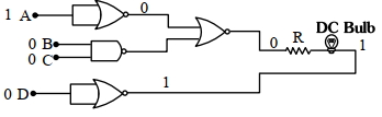
The following logic gate circuit is connected in a suitable arrangement. For which of the following combinations will the bulb glow $(ON)$?
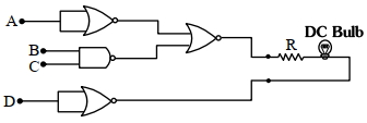
A
$A=0, B=1, C=1, D=1$
B
$A=1, B=0, C=0, D=0$
C
$A=0, B=0, C=0, D=1$
D
$A=1, B=1, C=1, D=0$
Solution
(B) The bulb will glow if there is a potential difference across it. This means one end of the bulb must be at a high potential $(1)$ and the other end must be at a low potential $(0)$.
Let $X$ be the output of the first $NOR$ gate,$Y$ be the output of the $NAND$ gate,and $Z$ be the output of the final $NOR$ gate connected to the resistor.
$X = \overline{A+A} = \overline{A}$
$Y = \overline{B \cdot C}$
$Z = \overline{X+Y} = \overline{\overline{A} + \overline{B \cdot C}} = A \cdot (B \cdot C) = A \cdot B \cdot C$
Let $W$ be the output of the bottom $NOR$ gate: $W = \overline{D+D} = \overline{D}$.
The bulb glows if the potential difference between $Z$ and $W$ is $1$,i.e.,$(Z=1, W=0)$ or $(Z=0, W=1)$.
Checking option $(B)$: $A=1, B=0, C=0, D=0$.
$Z = 1 \cdot 0 \cdot 0 = 0$
$W = \overline{0} = 1$
Since $Z=0$ and $W=1$,there is a potential difference,so the bulb will glow.
0 likes
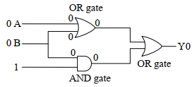
View Solution292
DifficultMCQ
The output $(Y)$ of the logic circuit given below is $0$ only when:
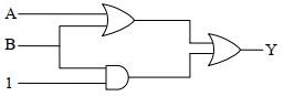
A
$A=1, B=0$
B
$A=0, B=0$
C
$A=1, B=1$
D
$A=0, B=1$
Solution
(B) The given circuit consists of an $OR$ gate,an $AND$ gate,and a final $OR$ gate.
Let the inputs be $A$ and $B$. The third input is fixed at $1$.
The output of the first $OR$ gate is $(A + B)$.
The output of the $AND$ gate is $(B \cdot 1) = B$.
The final output $Y$ is the $OR$ operation of these two outputs:
$Y = (A + B) + B$
Using Boolean algebra laws,specifically the idempotent law $(B + B = B)$,we simplify the expression:
$Y = A + (B + B) = A + B$
We want the output $Y$ to be $0$. For an $OR$ gate,the output is $0$ only if all inputs are $0$.
Therefore,$A + B = 0$ implies $A = 0$ and $B = 0$.
Thus,the output is $0$ when $A = 0$ and $B = 0$.
0 likes
View Solution293
DifficultMCQ
The correct truth table for the following logic circuit is:
A
| $A$ | $B$ | $Y$ |
| $0$ | $0$ | $0$ |
| $0$ | $1$ | $1$ |
| $1$ | $0$ | $0$ |
| $1$ | $1$ | $1$ |
B
| $A$ | $B$ | $Y$ |
| $0$ | $0$ | $1$ |
| $0$ | $1$ | $1$ |
| $1$ | $0$ | $0$ |
| $1$ | $1$ | $1$ |
C
| $A$ | $B$ | $Y$ |
| $0$ | $0$ | $1$ |
| $0$ | $1$ | $0$ |
| $1$ | $0$ | $0$ |
| $1$ | $1$ | $1$ |
D
| $A$ | $B$ | $Y$ |
| $0$ | $0$ | $0$ |
| $0$ | $1$ | $0$ |
| $1$ | $0$ | $0$ |
| $1$ | $1$ | $1$ |
Solution
(B) The given logic circuit consists of an $AND$ gate,a $NOT$ gate,and an $OR$ gate.
Input $A$ is connected to a $NOT$ gate,so its output is $\bar{A}$.
Inputs $A$ and $B$ are connected to an $AND$ gate,so its output is $A \cdot B$.
These two outputs are then fed into an $OR$ gate.
Therefore,the final output $Y$ is given by the Boolean expression: $Y = \bar{A} + (A \cdot B)$.
Using the distributive law of Boolean algebra,$Y = (\bar{A} + A) \cdot (\bar{A} + B)$.
Since $\bar{A} + A = 1$,we get $Y = 1 \cdot (\bar{A} + B) = \bar{A} + B$.
Now,let's construct the truth table for $Y = \bar{A} + B$:
- If $A=0, B=0$: $Y = \bar{0} + 0 = 1 + 0 = 1$.
- If $A=0, B=1$: $Y = \bar{0} + 1 = 1 + 1 = 1$.
- If $A=1, B=0$: $Y = \bar{1} + 0 = 0 + 0 = 0$.
- If $A=1, B=1$: $Y = \bar{1} + 1 = 0 + 1 = 1$.
Comparing this with the given options,option $B$ matches the calculated truth table.
0 likes
View Solution294
DifficultMCQ
The output $Y$ of the following circuit for given inputs $A$ and $B$ is:
A
$A \cdot B(A+B)$
B
$A \cdot B$
C
$0$
D
$\bar{A} \cdot B$
Solution
(C) Let the inputs be $A$ and $B$. The circuit consists of an $OR$ gate,an $AND$ gate,and two $NOT$ gates.
$1$. The upper part has an $OR$ gate with inputs $A$ and $\bar{B}$. Its output is $(A + \bar{B})$.
$2$. The lower part has an $AND$ gate with inputs $B$ and $\bar{A}$. Its output is $(B \cdot \bar{A})$.
$3$. The final output $Y$ is the $AND$ operation of these two outputs: $Y = (A + \bar{B}) \cdot (B \cdot \bar{A})$.
$4$. Expanding this expression: $Y = (A \cdot B \cdot \bar{A}) + (\bar{B} \cdot B \cdot \bar{A})$.
$5$. Since $A \cdot \bar{A} = 0$ and $B \cdot \bar{B} = 0$,we get $Y = 0 + 0 = 0$.
Thus,the output $Y$ is always $0$.
0 likes
View Solution295
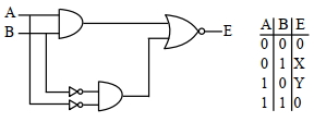
DifficultMCQ
In the truth table of the given circuit,the values of $X$ and $Y$ are:
A
$1, 1$
B
$1, 0$
C
$0, 1$
D
$0, 0$
Solution
(A) The given circuit consists of an $AND$ gate,two $NOT$ gates,another $AND$ gate,and a $NOR$ gate.
Let the inputs be $A$ and $B$. The output of the first $AND$ gate is $A \cdot B$.
The inputs to the second $AND$ gate are $\bar{A}$ and $\bar{B}$,so its output is $\bar{A} \cdot \bar{B}$.
These two outputs are fed into a $NOR$ gate,so the final output $E$ is $\overline{(A \cdot B) + (\bar{A} \cdot \bar{B})}$.
For $X$: $A = 0, B = 1$.
$E = \overline{(0 \cdot 1) + (\bar{0} \cdot \bar{1})} = \overline{0 + (1 \cdot 0)} = \overline{0 + 0} = \overline{0} = 1$. Thus,$X = 1$.
For $Y$: $A = 1, B = 0$.
$E = \overline{(1 \cdot 0) + (\bar{1} \cdot \bar{0})} = \overline{0 + (0 \cdot 1)} = \overline{0 + 0} = \overline{0} = 1$. Thus,$Y = 1$.
Therefore,the values of $X$ and $Y$ are $1, 1$.
0 likes
View Solution296
MediumMCQ
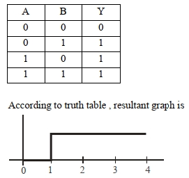
The output $(Y)$ of the given logic gate is similar to the output of an/a
A
$NOR$ gate
B
$OR$ gate
C
$AND$ gate
D
$NAND$ gate
Solution
(C) Let the inputs to the first $NAND$ gate be $A$ and $A$. The output is $Y_1 = \overline{A \cdot A} = \bar{A}$.
Let the inputs to the $NOR$ gate be $B$ and $B$. The output is $Y_2 = \overline{B+B} = \bar{B}$.
The final gate is a $NOR$ gate with inputs $Y_1$ and $Y_2$. The output $Y$ is given by:
$Y = \overline{Y_1 + Y_2}$
Substituting the values of $Y_1$ and $Y_2$:
$Y = \overline{\bar{A} + \bar{B}}$
Using De Morgan's theorem,$\overline{\bar{A} + \bar{B}} = \overline{\bar{A}} \cdot \overline{\bar{B}} = A \cdot B$.
Thus,the output $Y = A \cdot B$,which is the output of an $AND$ gate.
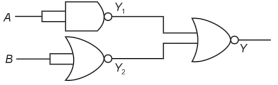
0 likes
View SolutionSemiconductor Electronics — Boolean Algebra and Logic Gates · Frequently Asked Questions
1Are these Semiconductor Electronics questions useful for JEE and NEET?
Yes. All questions in this section are mapped to JEE Main and NEET exam patterns. Previous year questions from JEE Main, NEET, GUJCET and state-level exams are included with full solutions.
2Can I switch to Hindi or Gujarati for these questions?
Yes. Use the language tabs in the hero section or the sidebar to view the same questions and solutions in English, Hindi or Gujarati.
3How do I generate a question paper from this subtopic?
Use the Vedclass Exam Paper Generator — select the chapter and subtopic, set difficulty, and generate Sets A, B, C, D automatically. First 3 chapters of every subject are free.
Vedclass Products
For Students
Vedclass Test Series
Mock tests in real JEE/NEET style with performance analysis. 5-day free trial.
Start Free TrialFor Teachers
Exam Paper Generator
Generate Set A/B/C/D papers from this chapter in 2 minutes. 3 chapters free.
Try FreeFor Institutes
Online Exam Module
Live online exams with unlimited students, 360° analytics & white-label branding.
See DemoFor Teachers & Institutes
Generate a Semiconductor Electronics Exam Paper in 2 Minutes
Select subtopic & difficulty — Sets A, B, C, D auto-generated with No Repeat logic.
First 3 chapters of every subject are free — no payment required.