
A English
Boolean Algebra and Logic Gates Questions in English
Class 12 Physics · Semiconductor Electronics · Boolean Algebra and Logic Gates
483+
Questions
English
Language
100%
With Solutions
Showing 47 of 483 questions in English
201
MediumMCQ
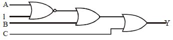
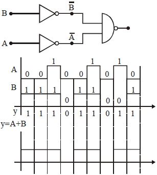
The expression for $Y$ in the following circuit is
A
$A+B+C$
B
$A+B \cdot C$
C
$B+C$
D
$1$
Solution
(C) $1$. The first gate is a $NOR$ gate with inputs $A$ and $1$. The output of this $NOR$ gate is $\overline{A+1}$. Since $A+1 = 1$,the output is $\overline{1} = 0$.
$2$. The second gate is an $OR$ gate with inputs from the first gate (which is $0$) and input $B$. The output of this $OR$ gate is $0+B = B$.
$3$. The third gate is an $OR$ gate with inputs from the second gate (which is $B$) and input $C$. The output $Y$ is $B+C$.
$2$. The second gate is an $OR$ gate with inputs from the first gate (which is $0$) and input $B$. The output of this $OR$ gate is $0+B = B$.
$3$. The third gate is an $OR$ gate with inputs from the second gate (which is $B$) and input $C$. The output $Y$ is $B+C$.
0 likes
View Solution202
MediumMCQ
Which of the following gates will have an output of $1$?
A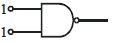
B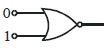
C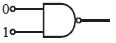
D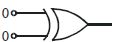
Solution
(C) Let us analyze each gate:
$(A)$ $NAND$ gate with inputs $1, 1$: Output $X = \overline{1 \cdot 1} = \overline{1} = 0$.
$(B)$ $NOR$ gate with inputs $0, 1$: Output $X = \overline{0 + 1} = \overline{1} = 0$.
$(C)$ $NAND$ gate with inputs $0, 1$: Output $X = \overline{0 \cdot 1} = \overline{0} = 1$.
$(D)$ $XOR$ gate with inputs $0, 0$: Output $X = 0 \oplus 0 = 0$.
Thus,the gate with an output of $1$ is the $NAND$ gate with inputs $0$ and $1$.
0 likes
View Solution203
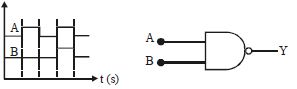
MediumMCQ
The input and the output waveforms of a logic gate are shown in the diagram. Identify the logic gate.
A
$AND$ gate
B
$OR$ gate
C
$NAND$ gate
D
$NOT$ gate
Solution
(A) By observing the waveforms at different time intervals,we can construct the truth table:
The truth table shows that the output $Y$ is $1$ only when both inputs $A$ and $B$ are $1$. This is the characteristic behavior of an $AND$ gate.
| Time Interval | Input $A$ | Input $B$ | Output $Y$ |
|---|---|---|---|
| $0 - T_1$ | $0$ | $0$ | $0$ |
| $T_1 - T_2$ | $0$ | $1$ | $0$ |
| $T_2 - T_3$ | $1$ | $0$ | $0$ |
| $T_3 - T_4$ | $1$ | $1$ | $1$ |
The truth table shows that the output $Y$ is $1$ only when both inputs $A$ and $B$ are $1$. This is the characteristic behavior of an $AND$ gate.
0 likes
View Solution204
MediumMCQ
An $AND$ gate
A
implements logic addition
B
is equivalent to a series switching circuit
C
is an any or all gate
D
is equivalent to a parallel switching circuit
Solution
(B) An $AND$ gate performs the logical multiplication operation. Its output is $1$ only if all its inputs are $1$.
In terms of switching circuits,an $AND$ gate is equivalent to two switches connected in series.
If both switches are closed (input $1$),current flows (output $1$). If either switch is open (input $0$),the circuit is broken (output $0$).
In terms of switching circuits,an $AND$ gate is equivalent to two switches connected in series.
If both switches are closed (input $1$),current flows (output $1$). If either switch is open (input $0$),the circuit is broken (output $0$).
0 likes
View Solution205
MediumMCQ
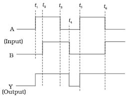
The following figure shows a logic gate circuit with two inputs $A$ and $B$ and the output $Y$. The voltage waveforms of $A$,$B$,and $Y$ are as given. The logic gate is:
A
$OR$
B
$AND$
C
$NAND$
D
$NOR$
Solution
(C) To identify the logic gate,we analyze the truth table derived from the given voltage waveforms:
From the truth table,we observe that the output $Y$ is $0$ only when both inputs $A$ and $B$ are $1$. In all other cases,the output is $1$. This behavior corresponds to the $NAND$ gate,which performs the operation $Y = \overline{AB}$.
| $A$ | $B$ | $Y$ |
|---|---|---|
| $1$ | $1$ | $0$ |
| $0$ | $0$ | $1$ |
| $0$ | $1$ | $1$ |
| $1$ | $0$ | $1$ |
From the truth table,we observe that the output $Y$ is $0$ only when both inputs $A$ and $B$ are $1$. In all other cases,the output is $1$. This behavior corresponds to the $NAND$ gate,which performs the operation $Y = \overline{AB}$.
0 likes
View Solution206
EasyMCQ
Which represents $NAND$ gate?
A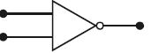
B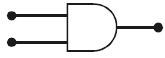
C
D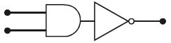
Solution
(D) $NAND$ gate is formed by connecting a $NOT$ gate to the output of an $AND$ gate.
In the given options,option $D$ shows an $AND$ gate followed by a $NOT$ gate,which is the standard representation of a $NAND$ gate.
In the given options,option $D$ shows an $AND$ gate followed by a $NOT$ gate,which is the standard representation of a $NAND$ gate.
0 likes
View Solution207
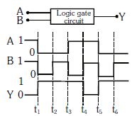
MediumMCQ
The real-time variation of input signals $A$ and $B$ are as shown below. If the inputs are fed into a $NAND$ gate,then select the output signal from the following.
A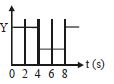
B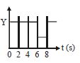
C
D
Solution
(B) $NAND$ gate produces an output of $0$ only when both inputs are $1$. Otherwise,it produces an output of $1$.
Based on the input waveforms for $A$ and $B$:
- For $t = 0$ to $2 \ s$: $A=0, B=0 \implies Y=1$.
- For $t = 2$ to $4 \ s$: $A=1, B=0 \implies Y=1$.
- For $t = 4$ to $6 \ s$: $A=0, B=0 \implies Y=1$.
- For $t = 6$ to $8 \ s$: $A=1, B=1 \implies Y=0$.
- For $t > 8 \ s$: $A=0, B=0 \implies Y=1$.
Comparing this sequence $(1, 1, 1, 0, 1)$ with the given options,the waveform in option $B$ matches this output.
0 likes
View Solution208
MediumMCQ
The following diagram performs the logic function of:
A
$XOR$ gate
B
$AND$ gate
C
$NAND$ gate
D
$OR$ gate
Solution
(B) The given circuit consists of two $NAND$ gates connected in series.
Let the inputs to the first $NAND$ gate be $A$ and $B$. The output of the first $NAND$ gate is $X = \overline{A \cdot B}$.
This output $X$ acts as the input to the second $NAND$ gate. Since both inputs of the second $NAND$ gate are connected to $X$, its output $Y$ is given by $Y = \overline{X \cdot X} = \overline{X}$.
Substituting the value of $X$, we get $Y = \overline{(\overline{A \cdot B})} = A \cdot B$.
The expression $Y = A \cdot B$ represents the logic function of an $AND$ gate.
Therefore, the given circuit performs the function of an $AND$ gate.
0 likes
View Solution209
EasyMCQ
Assertion: The logic gate $NOT$ can be built using a diode.
Reason: The output voltage and the input voltage of the diode have a $180^o$ phase difference.
Reason: The output voltage and the input voltage of the diode have a $180^o$ phase difference.
A
If both Assertion and Reason are correct and the Reason is a correct explanation of the Assertion.
B
If both Assertion and Reason are correct but Reason is not a correct explanation of the Assertion.
C
If the Assertion is correct but Reason is incorrect.
D
If both the Assertion and Reason are incorrect.
Solution
(D) $NOT$ gate is an inverter that requires an active component like a transistor to perform the inversion logic. $A$ diode is a passive,unidirectional device that allows current to flow in only one direction and cannot perform the logical inversion required for a $NOT$ gate.
Furthermore,a diode does not introduce a $180^o$ phase shift between the input and output voltages. Therefore,both the Assertion and the Reason are incorrect.
Furthermore,a diode does not introduce a $180^o$ phase shift between the input and output voltages. Therefore,both the Assertion and the Reason are incorrect.
0 likes
View Solution210
EasyMCQ
Assertion : $NAND$ or $NOR$ gates are called digital building blocks.
Reason : The repeated use of $NAND$ (or $NOR$) gates can produce all the basic or complicated gates.
Reason : The repeated use of $NAND$ (or $NOR$) gates can produce all the basic or complicated gates.
A
If both Assertion and Reason are correct and the Reason is a correct explanation of the Assertion.
B
If both Assertion and Reason are correct but Reason is not a correct explanation of the Assertion.
C
If the Assertion is correct but Reason is incorrect.
D
If both the Assertion and Reason are incorrect.
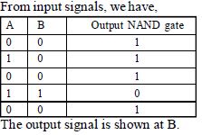
Solution
(A) $NAND$ and $NOR$ gates are known as universal gates or digital building blocks.
This is because any logic gate,such as $AND, OR, NOT, XOR,$ or $XNOR$,can be constructed using only $NAND$ gates or only $NOR$ gates.
Since the Assertion states they are building blocks and the Reason correctly explains that they can produce all other basic or complex gates,the Reason is the correct explanation of the Assertion.
0 likes
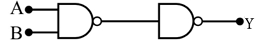
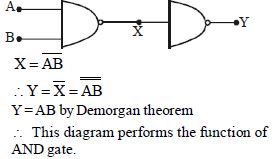
View Solution211
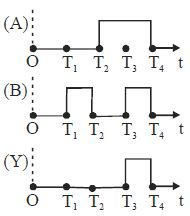
MediumMCQ
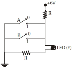
The correct Boolean operation represented by the circuit diagram shown is:
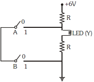
A
$AND$
B
$OR$
C
$NAND$
D
$NOR$
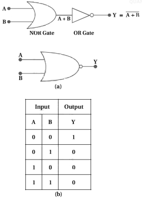
Solution
(C) In the given circuit,the switches $A$ and $B$ are connected in parallel with the ground. When a switch is at position $0$,it is open,and when it is at position $1$,it is closed (connected to ground).
$1$. If both $A=0$ and $B=0$,both switches are open. The current flows through the $LED$ $(Y)$,so $Y=1$.
$2$. If $A=0$ and $B=1$,switch $B$ is closed (grounded). The current flows through the $LED$ $(Y)$,so $Y=1$.
$3$. If $A=1$ and $B=0$,switch $A$ is closed (grounded). The current flows through the $LED$ $(Y)$,so $Y=1$.
$4$. If $A=1$ and $B=1$,both switches are closed (grounded). The current bypasses the $LED$ through the switches to the ground,so $Y=0$.
The truth table is:
This truth table corresponds to the $NAND$ gate operation.
$1$. If both $A=0$ and $B=0$,both switches are open. The current flows through the $LED$ $(Y)$,so $Y=1$.
$2$. If $A=0$ and $B=1$,switch $B$ is closed (grounded). The current flows through the $LED$ $(Y)$,so $Y=1$.
$3$. If $A=1$ and $B=0$,switch $A$ is closed (grounded). The current flows through the $LED$ $(Y)$,so $Y=1$.
$4$. If $A=1$ and $B=1$,both switches are closed (grounded). The current bypasses the $LED$ through the switches to the ground,so $Y=0$.
The truth table is:
| $A$ | $B$ | $Y$ |
|---|---|---|
| $0$ | $0$ | $1$ |
| $0$ | $1$ | $1$ |
| $1$ | $0$ | $1$ |
| $1$ | $1$ | $0$ |
This truth table corresponds to the $NAND$ gate operation.
0 likes
View Solution212
MediumMCQ
The circuit diagram shown here corresponds to which logic gate?
A
$NOR$
B
$AND$
C
$OR$
D
$NAND$
Solution
(A) In the given circuit,switches $A$ and $B$ are connected in parallel. The output $Y$ is the state of the $LED$.
When both switches $A$ and $B$ are at position $0$ (connected to ground),the $LED$ is connected across the $+6V$ supply through resistor $R$,so the $LED$ glows $(Y=1)$.
If either switch $A$ or $B$ is moved to position $1$,the circuit is shorted to ground,and the potential difference across the $LED$ becomes zero,so the $LED$ does not glow $(Y=0)$.
The truth table is:
This truth table corresponds to the $NOR$ gate.
When both switches $A$ and $B$ are at position $0$ (connected to ground),the $LED$ is connected across the $+6V$ supply through resistor $R$,so the $LED$ glows $(Y=1)$.
If either switch $A$ or $B$ is moved to position $1$,the circuit is shorted to ground,and the potential difference across the $LED$ becomes zero,so the $LED$ does not glow $(Y=0)$.
The truth table is:
| $A$ | $B$ | $Y$ |
| $0$ | $0$ | $1$ |
| $0$ | $1$ | $0$ |
| $1$ | $0$ | $0$ |
| $1$ | $1$ | $0$ |
This truth table corresponds to the $NOR$ gate.
0 likes
View Solution213
MediumMCQ
Which of the following gives a reversible operation?
A
B
C
D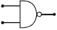
Solution
(B) logic gate is considered reversible if the input data can be uniquely recovered from the output data.
In a $NOT$ gate,the output is the complement of the input $(Y = \bar{A})$. If the output is $0$,the input must have been $1$,and if the output is $1$,the input must have been $0$. Thus,the input can be uniquely determined from the output.
Other gates like $OR$,$NOR$,$AND$,and $NAND$ have two inputs,meaning there are $2^2 = 4$ possible input combinations,but only $2$ possible output states ($0$ or $1$). Since multiple input combinations can produce the same output,these gates are not reversible.
0 likes
View Solution214
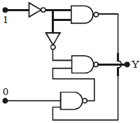
MediumMCQ
In the given circuit,find the value of $Y$.
A
will not execute
B
$0$
C
toggles between $0$ and $1$
D
$1$
Solution
(D) Let the inputs be $A=1$ and $B=0$.
$1$. The input $A=1$ passes through a $NOT$ gate,becoming $0$.
$2$. This $0$ is fed into the top $NAND$ gate (both inputs are $0$),so the output of the top $NAND$ gate is $\overline{0 \cdot 0} = 1$.
$3$. The $0$ from the first $NOT$ gate also passes through another $NOT$ gate,becoming $1$.
$4$. This $1$ is fed into the middle $NAND$ gate.
$5$. The bottom $NAND$ gate has inputs $B=0$ and the feedback from $Y$.
$6$. Analyzing the circuit,the output $Y$ is connected to the output of the top and middle $NAND$ gates.
$7$. Given the configuration,the output $Y$ stabilizes at $1$.
0 likes
View Solution215
MediumMCQ
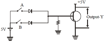
The Boolean relation at the output stage $Y$ for the following circuit is:
A
$A+B$
B
$\overline{A}+\overline{B}$
C
$\overline{A} \cdot \overline{B}$
D
$A \cdot B$
Solution
(C) The circuit consists of two switches $A$ and $B$ connected to diodes,which act as an $OR$ gate input stage. When either switch $A$ or $B$ is closed (logic $1$),the base of the $NPN$ transistor receives a high voltage,causing it to conduct. When the transistor conducts,the collector voltage drops to near $0 \ V$ (logic $0$). If both switches are open (logic $0$),the base is grounded through the resistor,the transistor is in cutoff $(OFF)$,and the output $Y$ is pulled up to $+5 \ V$ (logic $1$). This behavior corresponds to a $NOR$ gate,where $Y = \overline{A+B}$. According to De Morgan's theorem,$\overline{A+B} = \overline{A} \cdot \overline{B}$.
| $A$ | $B$ | $Y$ |
| $0$ | $0$ | $1$ |
| $1$ | $0$ | $0$ |
| $0$ | $1$ | $0$ |
| $1$ | $1$ | $0$ |
0 likes
View Solution216
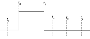
Medium
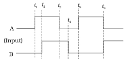
Justify the output waveform $(Y)$ of the $OR$ gate for the following inputs $A$ and $B$ given in the figure.
Solution
(N/A) For an $OR$ gate,the output $Y = A + B$. This means the output is $1$ if either input $A$ or $B$ is $1$,and $0$ only if both inputs are $0$.
$1$. For $t < t_{1}$: $A=0, B=0$,so $Y = 0 + 0 = 0$.
$2$. For $t_{1}$ to $t_{2}$: $A=1, B=0$,so $Y = 1 + 0 = 1$.
$3$. For $t_{2}$ to $t_{3}$: $A=1, B=1$,so $Y = 1 + 1 = 1$.
$4$. For $t_{3}$ to $t_{4}$: $A=0, B=1$,so $Y = 0 + 1 = 1$.
$5$. For $t_{4}$ to $t_{5}$: $A=0, B=0$,so $Y = 0 + 0 = 0$.
$6$. For $t_{5}$ to $t_{6}$: $A=1, B=0$,so $Y = 1 + 0 = 1$.
$7$. For $t > t_{6}$: $A=0, B=1$,so $Y = 0 + 1 = 1$.
Thus,the output waveform $Y$ follows the logic of the $OR$ gate as shown in the figure.
0 likes
View Solution217
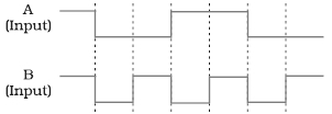
Medium
Consider the input waveforms $A$ and $B$ as shown in the figure. Sketch the output waveform obtained from an $AND$ gate.
Solution
(N/A) For an $AND$ gate,the output $Y$ is $1$ only when both inputs $A$ and $B$ are $1$. Otherwise,the output $Y$ is $0$. Based on the provided input waveforms,we analyze the intervals:
Thus,the output waveform remains at a low state $(0)$ for all intervals except between $t_{2}$ and $t_{3}$,where it goes to a high state $(1)$.
| Interval | Inputs $(A, B)$ | Output $(Y = A \cdot B)$ |
| $t \leq t_{1}$ | $A=0, B=0$ | $Y=0$ |
| $t_{1}$ to $t_{2}$ | $A=1, B=0$ | $Y=0$ |
| $t_{2}$ to $t_{3}$ | $A=1, B=1$ | $Y=1$ |
| $t_{3}$ to $t_{4}$ | $A=0, B=1$ | $Y=0$ |
| $t_{4}$ to $t_{5}$ | $A=0, B=0$ | $Y=0$ |
| $t_{5}$ to $t_{6}$ | $A=1, B=0$ | $Y=0$ |
| $t > t_{6}$ | $A=0, B=0$ | $Y=0$ |
Thus,the output waveform remains at a low state $(0)$ for all intervals except between $t_{2}$ and $t_{3}$,where it goes to a high state $(1)$.
0 likes
View Solution218
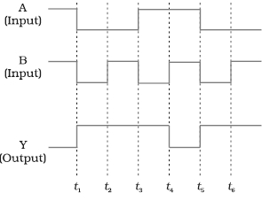
Medium
Sketch the output $Y$ from a $NAND$ gate having inputs $A$ and $B$ as shown in the figure.
Solution
(N/A) The truth table for a $NAND$ gate is:
If $A=0, B=0$,then $Y=1$.
If $A=0, B=1$,then $Y=1$.
If $A=1, B=0$,then $Y=1$.
If $A=1, B=1$,then $Y=0$.
Based on the input waveforms:
For $t < t_{1}$; $A=1, B=1$; hence $Y=0$.
For $t_{1}$ to $t_{2}$; $A=0, B=0$; hence $Y=1$.
For $t_{2}$ to $t_{3}$; $A=0, B=1$; hence $Y=1$.
For $t_{3}$ to $t_{4}$; $A=1, B=0$; hence $Y=1$.
For $t_{4}$ to $t_{5}$; $A=1, B=1$; hence $Y=0$.
For $t_{5}$ to $t_{6}$; $A=0, B=0$; hence $Y=1$.
For $t > t_{6}$; $A=1, B=1$; hence $Y=0$.
0 likes
View Solution219
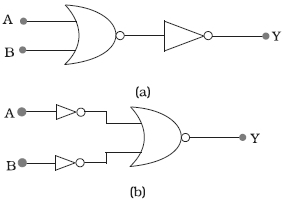
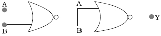
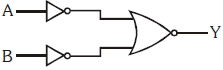
Medium
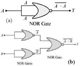
You are given two circuits as shown in the figure. Show that circuit $(a)$ acts as an $OR$ gate while circuit $(b)$ acts as an $AND$ gate.
Solution
(N/A) and $B$ are the inputs and $Y$ is the output of the given circuit. The left part of the circuit is a $NOR$ gate,and the right part is a $NOT$ gate.
The output of the $NOR$ gate is $\overline{A+B}$.
This output serves as the input for the $NOT$ gate. The output of the $NOT$ gate is $\overline{\overline{A+B}} = A+B$.
Therefore,$Y = A+B$,which is the Boolean expression for an $OR$ gate. Hence,this circuit functions as an $OR$ gate.
$(b)$ $A$ and $B$ are the inputs and $Y$ is the output. The inputs $A$ and $B$ first pass through two $NOT$ gates,producing $\overline{A}$ and $\overline{B}$ respectively.
These are then fed as inputs to a $NOR$ gate.
The output of the $NOR$ gate is $Y = \overline{\overline{A} + \overline{B}}$.
Using De Morgan's theorem,$\overline{\overline{A} + \overline{B}} = \overline{\overline{A}} \cdot \overline{\overline{B}} = A \cdot B$.
Therefore,$Y = A \cdot B$,which is the Boolean expression for an $AND$ gate. Hence,this circuit functions as an $AND$ gate.
0 likes
View Solution220
Easy
Write the truth table for a $NAND$ gate connected as given in the figure. Hence,identify the exact logic operation carried out by this circuit.
Solution
(N/A) In the given circuit,the input $A$ is connected to both inputs of the $NAND$ gate. Let the inputs be $A_1 = A$ and $A_2 = A$. The output $Y$ of a $NAND$ gate is given by $Y = \overline{A_1 \cdot A_2}$.
Substituting the inputs,we get:
$Y = \overline{A \cdot A}$
Using the Boolean identity $A \cdot A = A$,we have:
$Y = \overline{A}$
The truth table for this operation is:
Since the output $Y$ is the complement of the input $A$,this circuit functions as a $NOT$ gate.
Substituting the inputs,we get:
$Y = \overline{A \cdot A}$
Using the Boolean identity $A \cdot A = A$,we have:
$Y = \overline{A}$
The truth table for this operation is:
| $A$ | $Y = \overline{A}$ |
|---|---|
| $0$ | $1$ |
| $1$ | $0$ |
Since the output $Y$ is the complement of the input $A$,this circuit functions as a $NOT$ gate.
0 likes
View Solution221
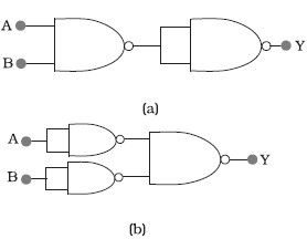
Medium
You are given two circuits as shown in the figure,which consist of $NAND$ gates. Identify the logic operation carried out by the two circuits.
Solution
(N/A) In both the given circuits,$A$ and $B$ are the inputs and $Y$ is the output.
$(a)$ The output of the first $NAND$ gate is $\overline{A \cdot B}$. This output is fed into a second $NAND$ gate where both inputs are connected together. $A$ $NAND$ gate with both inputs connected acts as a $NOT$ gate. Therefore,the final output is $Y = \overline{(\overline{A \cdot B})} = A \cdot B$. Hence,this circuit functions as an $AND$ gate.
$(b)$ In this circuit,the first two $NAND$ gates have their inputs connected together,so they act as $NOT$ gates. The outputs are $\overline{A}$ and $\overline{B}$ respectively. These are then fed into a third $NAND$ gate. The final output is $Y = \overline{\overline{A} \cdot \overline{B}}$. By De Morgan's theorem,$\overline{\overline{A} \cdot \overline{B}} = \overline{\overline{A}} + \overline{\overline{B}} = A + B$. Hence,this circuit functions as an $OR$ gate.
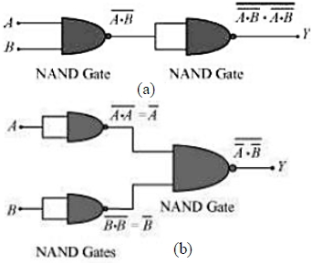
0 likes
View Solution222
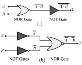
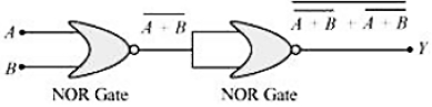
Medium
Write the truth table for the circuit given in the figure below,which consists of $NOR$ gates,and identify the logic operation $(OR, AND, NOT)$ that this circuit performs.
Solution
(N/A) Let $A$ and $B$ be the inputs of the given circuit. The output of the first $NOR$ gate is $\overline{A+B}$.
It can be observed from the figure that the output of the first $NOR$ gate acts as the input for both terminals of the second $NOR$ gate.
Therefore,the final output $Y$ is given by:
$Y = \overline{(\overline{A+B}) + (\overline{A+B})}$
Using the Boolean identity $\overline{X+X} = \overline{X}$,we get:
$Y = \overline{(\overline{A+B})} = A+B$
The truth table for this operation is:
This is the truth table of an $OR$ gate. Hence,this circuit functions as an $OR$ gate.
It can be observed from the figure that the output of the first $NOR$ gate acts as the input for both terminals of the second $NOR$ gate.
Therefore,the final output $Y$ is given by:
$Y = \overline{(\overline{A+B}) + (\overline{A+B})}$
Using the Boolean identity $\overline{X+X} = \overline{X}$,we get:
$Y = \overline{(\overline{A+B})} = A+B$
The truth table for this operation is:
| $A$ | $B$ | $Y (= A + B)$ |
|---|---|---|
| $0$ | $0$ | $0$ |
| $0$ | $1$ | $1$ |
| $1$ | $0$ | $1$ |
| $1$ | $1$ | $1$ |
This is the truth table of an $OR$ gate. Hence,this circuit functions as an $OR$ gate.
0 likes
View Solution223
Medium
Identify the logic gates represented by the given circuits $(a)$ and $(b)$ and write their truth tables.
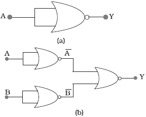
Solution
(N/A) For circuit $(a)$:
Input $A$ is connected to both inputs of the $NOR$ gate. The output $Y$ is given by $Y = \overline{A+A} = \bar{A}$.
The truth table is:
This is the truth table of a $NOT$ gate. Hence,circuit $(a)$ functions as a $NOT$ gate.
For circuit $(b)$:
$A$ and $B$ are inputs. The first two $NOR$ gates act as $NOT$ gates,producing outputs $\bar{A}$ and $\bar{B}$.
These are inputs to the final $NOR$ gate. The output $Y$ is:
$Y = \overline{\bar{A}+\bar{B}} = \overline{\overline{A \cdot B}} = A \cdot B$ (using De Morgan's theorem).
The truth table is:
This is the truth table of an $AND$ gate. Hence,circuit $(b)$ functions as an $AND$ gate.
Input $A$ is connected to both inputs of the $NOR$ gate. The output $Y$ is given by $Y = \overline{A+A} = \bar{A}$.
The truth table is:
| $A$ | $Y(=\bar{A})$ |
| $0$ | $1$ |
| $1$ | $0$ |
This is the truth table of a $NOT$ gate. Hence,circuit $(a)$ functions as a $NOT$ gate.
For circuit $(b)$:
$A$ and $B$ are inputs. The first two $NOR$ gates act as $NOT$ gates,producing outputs $\bar{A}$ and $\bar{B}$.
These are inputs to the final $NOR$ gate. The output $Y$ is:
$Y = \overline{\bar{A}+\bar{B}} = \overline{\overline{A \cdot B}} = A \cdot B$ (using De Morgan's theorem).
The truth table is:
| $A$ | $B$ | $Y(=A \cdot B)$ |
| $0$ | $0$ | $0$ |
| $0$ | $1$ | $0$ |
| $1$ | $0$ | $0$ |
| $1$ | $1$ | $1$ |
This is the truth table of an $AND$ gate. Hence,circuit $(b)$ functions as an $AND$ gate.
0 likes
View Solution224
EasyMCQ
The Boolean equation of a logic gate is $Y = \bar{A} \cdot B + A \cdot \bar{B}$. Identify the logic gate and describe its construction using $OR$,$AND$,and $NOT$ gates.
A
$AND$ gate
B
$OR$ gate
C
$XOR$ gate
D
$NAND$ gate
Solution
(C) The given Boolean expression is $Y = \bar{A} \cdot B + A \cdot \bar{B}$.
This is the standard Boolean expression for an $XOR$ (Exclusive $OR$) gate.
To construct this using basic gates:
$1$. Use two $NOT$ gates to obtain $\bar{A}$ and $\bar{B}$ from inputs $A$ and $B$.
$2$. Use two $AND$ gates: the first $AND$ gate takes inputs $\bar{A}$ and $B$ to produce $\bar{A} \cdot B$. The second $AND$ gate takes inputs $A$ and $\bar{B}$ to produce $A \cdot \bar{B}$.
$3$. Use one $OR$ gate to combine the outputs of the two $AND$ gates: $Y = (\bar{A} \cdot B) + (A \cdot \bar{B})$.
0 likes
View Solution225
Medium
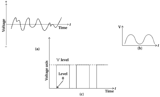
What are analog signals and digital signals?
Solution
(N/A) In electronic circuits such as amplifiers and oscillators,signals exist in the form of continuous changes in current or voltage over time. Such signals are called continuous or analog signals.
$A$ typical analog signal is shown in figures $(a)$ and $(b)$.
If a current or voltage signal has only two discrete values (minimum and maximum),the signal is called a digital signal.
The signal in figure $(c)$ is in the form of a waveform or pulse,which has only two signal levels.
$A$ binary system for displaying such signals is convenient. Binary uses only two digits,$0$ and $1$. The maximum value (e.g.,$5 \ V$) of voltage is expressed as $1$,and the minimum value (e.g.,$0 \ V$) is expressed as $0$.
The input and output voltages indicated by these two values ($0$ and $1$) in a digital circuit are valid.
0 likes
View Solution226
Medium
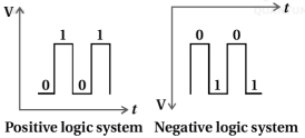
Explain the types of logic systems used in digital electronics.
Solution
(N/A) There are two types of systems used in logic circuits:
$(1)$ Positive logic system: In this type of system,the higher voltage level is assigned as logic $'1'$ (high) and the lower voltage level is assigned as logic $'0'$ (low).
$(2)$ Negative logic system: In this type of system,the lower voltage level is assigned as logic $'1'$ (high) and the higher voltage level is assigned as logic $'0'$ (low).
0 likes
View Solution227
Medium
Explain logic gates.
Solution
(N/A) logic gate is a digital circuit that implements a specific logical function. It operates based on a defined logical relationship between the input and output voltages.
They are called 'gates' because they control the flow of information based on logical conditions.
The five common logic gates are $NOT$,$AND$,$OR$,$NAND$,and $NOR$. Each logic gate is represented by a unique symbol,and its behavior is defined by its truth table.
$A$ truth table is a table that lists all possible input combinations and their corresponding output values for a logic gate.
The Boolean expression provides the mathematical representation of the operation performed by a specific logic gate.
Logic gates are constructed using semiconductor devices,such as diodes and transistors.
0 likes
View Solution228
Medium
Write the symbol,truth table,function,and Boolean equation for $NOT$,$AND$,and $OR$ gates.
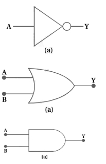
Solution
(N/A) $NOT$ Gate:
Symbol: Shown in figure $(a)$. It has one input $A$ and one output $Y$.
Function: If input is $1$,output is $0$. If input is $0$,output is $1$. It acts as an inverter.
Boolean Equation: $Y = \overline{A}$.
Truth Table:
| Input $A$ | Output $Y$ |
| :--- | :--- |
| $0$ | $1$ |
| $1$ | $0$ |
$OR$ Gate:
Symbol: Shown in figure $(a)$. It has two or more inputs $(A, B)$ and one output $Y$.
Function: The output is $1$ if at least one input is $1$.
Boolean Equation: $Y = A + B$.
Truth Table:
| Input $A$ | Input $B$ | Output $Y$ |
| :--- | :--- | :--- |
| $0$ | $0$ | $0$ |
| $0$ | $1$ | $1$ |
| $1$ | $0$ | $1$ |
| $1$ | $1$ | $1$ |
$AND$ Gate:
Symbol: Shown in figure $(a)$. It has two or more inputs $(A, B)$ and one output $Y$.
Function: The output is $1$ only if both inputs $A$ and $B$ are $1$.
Boolean Equation: $Y = A \bullet B$.
Truth Table:
| Input $A$ | Input $B$ | Output $Y$ |
| :--- | :--- | :--- |
| $0$ | $0$ | $0$ |
| $0$ | $1$ | $0$ |
| $1$ | $0$ | $0$ |
| $1$ | $1$ | $1$ |
0 likes
View Solution229
Medium
What are $NAND$ and $NOR$ gates? Write their symbols,truth tables,functions,and Boolean equations.
Solution
(N/A) $NAND$ gate is constructed by combining an $AND$ gate and a $NOT$ gate. $\therefore AND + NOT = NAND$.
This is an $AND$ gate followed by a $NOT$ gate. The symbol of this gate is represented by an $AND$ gate with a small circle at the output. It has two inputs $(A, B)$ and one output $(Y)$.
Function of $NAND$ gate: The output is $'0'$ only when all inputs are $'1'$,otherwise the output is $'1'$.
Boolean equation: $Y = \overline{A \cdot B}$.
Truth Table for $NAND$ gate:
| $A$ | $B$ | $Y$ |
|---|---|---|
| $0$ | $0$ | $1$ |
| $0$ | $1$ | $1$ |
| $1$ | $0$ | $1$ |
| $1$ | $1$ | $0$ |
$NAND$ gates are called universal gates because they can be used to realize other basic gates like $OR$,$AND$,and $NOT$.
$NOR$ gate is constructed by combining an $OR$ gate and a $NOT$ gate. $\therefore OR + NOT = NOR$.
This is an $OR$ gate followed by a $NOT$ gate. The symbol is an $OR$ gate with a small circle at the output.
Function of $NOR$ gate: The output is $'1'$ only when all inputs are $'0'$,otherwise the output is $'0'$.
Boolean equation: $Y = \overline{A + B}$.
Truth Table for $NOR$ gate:
| $A$ | $B$ | $Y$ |
|---|---|---|
| $0$ | $0$ | $1$ |
| $0$ | $1$ | $0$ |
| $1$ | $0$ | $0$ |
| $1$ | $1$ | $0$ |
$NOR$ gates are also called universal gates.
0 likes
View Solution230
Medium
What is a digital signal? What mathematical method is used to express it?
Solution
(N/A) digital signal is a signal that can take only two discrete values,typically represented as $0$ (low) and $1$ (high). These values correspond to specific voltage levels in electronic circuits.
The mathematical method used to express digital signals is known as $Boolean$ $Algebra$. It is a branch of algebra in which the values of the variables are the truth values $true$ and $false$,usually denoted by $1$ and $0$ respectively.
The mathematical method used to express digital signals is known as $Boolean$ $Algebra$. It is a branch of algebra in which the values of the variables are the truth values $true$ and $false$,usually denoted by $1$ and $0$ respectively.
0 likes
View Solution231
MediumMCQ
What is a logic gate?
A
$A$ device that stores electrical charge.
B
$A$ digital circuit that follows certain logical relationships between input and output voltages.
C
$A$ device used to amplify weak signals.
D
$A$ component used to convert $AC$ to $DC$.
Solution
(B) logic gate is a fundamental building block of a digital circuit. It is a digital circuit that performs a logical operation on one or more binary inputs and produces a single binary output. The relationship between the input and output is based on certain logical rules,which are represented by Boolean algebra. Common examples include $AND$,$OR$,$NOT$,$NAND$,and $NOR$ gates.
0 likes
View Solution232
MediumMCQ
What is the logic gate with one input and one output?
A
$AND$ gate
B
$OR$ gate
C
$NOT$ gate
D
$NAND$ gate
Solution
(C) logic gate is a digital circuit that performs a logical operation on one or more inputs and produces a single output.
Among the basic logic gates,the $NOT$ gate is the only one that has exactly one input and one output.
The $NOT$ gate performs the operation of inversion,meaning if the input is $0$,the output is $1$,and if the input is $1$,the output is $0$.
Therefore,the correct option is $C$.
Among the basic logic gates,the $NOT$ gate is the only one that has exactly one input and one output.
The $NOT$ gate performs the operation of inversion,meaning if the input is $0$,the output is $1$,and if the input is $1$,the output is $0$.
Therefore,the correct option is $C$.
0 likes
View Solution233
EasyMCQ
Which of the following is an inverter gate?
A
$AND$ gate
B
$OR$ gate
C
$NOT$ gate
D
$NAND$ gate
Solution
(C) An inverter gate is a logic gate that implements logical negation. It takes a single input and produces the opposite output. The $NOT$ gate is known as an inverter because if the input is $1$ (high),the output is $0$ (low),and if the input is $0$ (low),the output is $1$ (high). Therefore,the $NOT$ gate is the inverter gate.
0 likes
View Solution234
EasyMCQ
Write the function of $AND$ gate.
A
Output is $1$ if all inputs are $1$.
B
Output is $1$ if any input is $1$.
C
Output is $0$ if all inputs are $1$.
D
Output is $1$ if all inputs are $0$.
Solution
(A) The $AND$ gate is a basic digital logic gate that implements logical conjunction.
It produces an output of $1$ (high) only if all its inputs are $1$ (high).
If any of the inputs are $0$ (low),the output will be $0$ (low).
Mathematically,for two inputs $A$ and $B$,the output $Y$ is given by $Y = A \cdot B$.
It produces an output of $1$ (high) only if all its inputs are $1$ (high).
If any of the inputs are $0$ (low),the output will be $0$ (low).
Mathematically,for two inputs $A$ and $B$,the output $Y$ is given by $Y = A \cdot B$.
0 likes
View Solution235
Easy
Write the truth table of $NAND$ gate.
Solution
(N/A) $NAND$ gate is a universal logic gate that produces a low output $(0)$ only when all its inputs are high $(1)$. Otherwise, it produces a high output $(1)$.
For a two-input $NAND$ gate with inputs $A$ and $B$ and output $Y$, the Boolean expression is $Y = \overline{A \cdot B}$.
The truth table is as follows:
| Input $A$ | Input $B$ | Output $Y$ |
| :--- | :--- | :--- |
| $0$ | $0$ | $1$ |
| $0$ | $1$ | $1$ |
| $1$ | $0$ | $1$ |
| $1$ | $1$ | $0$ |
For a two-input $NAND$ gate with inputs $A$ and $B$ and output $Y$, the Boolean expression is $Y = \overline{A \cdot B}$.
The truth table is as follows:
| Input $A$ | Input $B$ | Output $Y$ |
| :--- | :--- | :--- |
| $0$ | $0$ | $1$ |
| $0$ | $1$ | $1$ |
| $1$ | $0$ | $1$ |
| $1$ | $1$ | $0$ |
0 likes
View Solution236
EasyMCQ
The $NOR$ gate is a combination of which two gates?
A
$OR$ gate and $NOT$ gate
B
$AND$ gate and $NOT$ gate
C
$NAND$ gate and $OR$ gate
D
$OR$ gate and $AND$ gate
Solution
(A) $NOR$ gate is a universal logic gate that performs the logical $OR$ operation followed by the logical $NOT$ operation.
Therefore, the output of a $NOR$ gate is the complement of the output of an $OR$ gate.
Mathematically, if the inputs are $A$ and $B$, the output $Y$ is given by $Y = \overline{A + B}$.
This is equivalent to an $OR$ gate connected in series with a $NOT$ gate.
Therefore, the output of a $NOR$ gate is the complement of the output of an $OR$ gate.
Mathematically, if the inputs are $A$ and $B$, the output $Y$ is given by $Y = \overline{A + B}$.
This is equivalent to an $OR$ gate connected in series with a $NOT$ gate.
0 likes
View Solution237
Easy
What are basic gates and universal gates?
Solution
(N/A) Basic gates are the fundamental building blocks of digital logic circuits. They perform simple logical operations. The three basic logic gates are:
$1$. $NOT$ gate: It acts as an inverter,producing an output that is the inverse of the input.
$2$. $AND$ gate: It produces a high output $(1)$ only if all its inputs are high $(1)$.
$3$. $OR$ gate: It produces a high output $(1)$ if at least one of its inputs is high $(1)$.
Universal gates are logic gates that can be used to implement any Boolean function or construct any other type of logic gate without the need for other types of gates. The two universal gates are:
$1$. $NAND$ gate: It is a combination of an $AND$ gate followed by a $NOT$ gate.
$2$. $NOR$ gate: It is a combination of an $OR$ gate followed by a $NOT$ gate.
0 likes
View Solution238
Medium
Two car garages have a common gate which needs to open automatically when a car enters either of the garages or cars enter both. Devise a circuit that resembles this situation using diodes.
Solution
(N/A) In this scenario,the gate needs to open if input $A$ is high $OR$ input $B$ is high. This logic corresponds to an $OR$ gate. $A$ diode-based $OR$ gate circuit is used here,where the cathodes of two diodes are connected together to the output $C$,and the anodes serve as inputs $A$ and $B$. When either input $A$ or $B$ is at a high potential (logic $1$),the corresponding diode becomes forward-biased,allowing current to flow and raising the potential at output $C$ to a high state (logic $1$). If both are high,the output remains high. If both are low (logic $0$),the output is low.
Truth table for $OR$ gate:
Truth table for $OR$ gate:
| Inputs $(A, B)$ | Output $(C)$ |
| $0, 0$ | $0$ |
| $0, 1$ | $1$ |
| $1, 0$ | $1$ |
| $1, 1$ | $1$ |
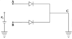
0 likes
View Solution239
Difficult
How would you set up a circuit to obtain a $NOT$ gate using a transistor?
Solution
(N/A) To obtain a $NOT$ gate using an $NPN$ transistor, the transistor is used in the common-emitter configuration. The input $A$ is applied to the base through a resistor $R_B$, and the output $C$ is taken from the collector terminal.
For case $I$:
When $A=0$ (low input), the base current $I_B = 0$. Consequently, the collector current $I_C = \beta I_B = 0$. Using Kirchhoff's voltage law in the output loop, $V_{CC} = I_C R_C + V_{CE}$. Since $I_C = 0$, $V_{CE} = V_{CC} = 5 \text{ V}$. Thus, the output $C = 1$ (high).
For case $II$:
When $A=1$ (high input), the transistor is driven into saturation, making $I_B$ and $I_C$ maximum. In this state, the voltage drop across $R_C$ is nearly equal to $V_{CC}$, so $V_{CE} \approx 0$. Thus, the output $C = 0$ (low).
This confirms the operation $C = \bar{A}$, which is the characteristic of a $NOT$ gate.
| Input $A$ | Output $C$ |
| $0$ | $1$ |
| $1$ | $0$ |
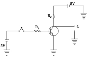
0 likes
View Solution240
Medium
Write the truth table for the circuit shown in the figure. Name the gate that the circuit resembles.
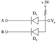
Solution
(N/A) The given circuit is an $OR$ gate.
When input $A$ or input $B$ is at a low potential $(0)$,the corresponding diode ($D_1$ or $D_2$) becomes forward-biased and conducts,pulling the output $V_0$ to a low potential $(0)$.
When both inputs $A$ and $B$ are at a high potential $(1)$,both diodes are reverse-biased and do not conduct. The output $V_0$ is then pulled to the high potential $(+5 \text{ V})$ through the resistor.
Thus,the circuit acts as an $OR$ gate.
The truth table is as follows:
| $A$ | $B$ | $V_0 = A + B$ |
|---|---|---|
| $0$ | $0$ | $0$ |
| $0$ | $1$ | $1$ |
| $1$ | $0$ | $1$ |
| $1$ | $1$ | $1$ |
0 likes
View Solution241
Medium
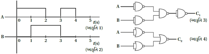
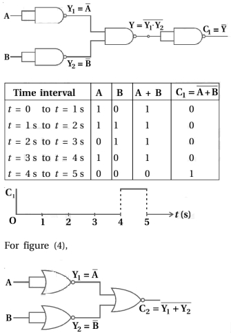
Draw the output signals $C_1$ and $C_2$ for the given combination of gates as shown in the figure.
Solution
(N/A) For the circuit in figure $(3)$:
$Y_1 = \overline{A}$,$Y_2 = \overline{B}$.
The output of the $NAND$ gate is $Y = \overline{Y_1 \cdot Y_2} = \overline{\overline{A} \cdot \overline{B}} = A + B$.
The final $NOT$ gate gives $C_1 = \overline{Y} = \overline{A + B}$.
This is the Boolean expression for a $NOR$ gate.
Based on the input signals $A$ and $B$,the output $C_1$ is high $(1)$ only when both $A$ and $B$ are low $(0)$,which occurs in the interval $t = 4 \text{ s}$ to $t = 5 \text{ s}$.
For the circuit in figure $(4)$:
$Y_1 = \overline{A}$,$Y_2 = \overline{B}$.
The output of the $NOR$ gate is $C_2 = \overline{Y_1 + Y_2} = \overline{\overline{A} + \overline{B}} = \overline{\overline{A \cdot B}} = A \cdot B$.
This is the Boolean expression for an $AND$ gate.
Based on the input signals $A$ and $B$,the output $C_2$ is high $(1)$ only when both $A$ and $B$ are high $(1)$,which occurs in the interval $t = 1 \text{ s}$ to $t = 2 \text{ s}$.
$Y_1 = \overline{A}$,$Y_2 = \overline{B}$.
The output of the $NAND$ gate is $Y = \overline{Y_1 \cdot Y_2} = \overline{\overline{A} \cdot \overline{B}} = A + B$.
The final $NOT$ gate gives $C_1 = \overline{Y} = \overline{A + B}$.
This is the Boolean expression for a $NOR$ gate.
Based on the input signals $A$ and $B$,the output $C_1$ is high $(1)$ only when both $A$ and $B$ are low $(0)$,which occurs in the interval $t = 4 \text{ s}$ to $t = 5 \text{ s}$.
For the circuit in figure $(4)$:
$Y_1 = \overline{A}$,$Y_2 = \overline{B}$.
The output of the $NOR$ gate is $C_2 = \overline{Y_1 + Y_2} = \overline{\overline{A} + \overline{B}} = \overline{\overline{A \cdot B}} = A \cdot B$.
This is the Boolean expression for an $AND$ gate.
Based on the input signals $A$ and $B$,the output $C_2$ is high $(1)$ only when both $A$ and $B$ are high $(1)$,which occurs in the interval $t = 1 \text{ s}$ to $t = 2 \text{ s}$.
0 likes
View Solution242
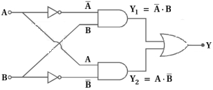
MediumMCQ
The truth table given below corresponds to which logic gate?
| $A$ | $B$ | $Y$ |
| $0$ | $0$ | $0$ |
| $0$ | $1$ | $1$ |
| $1$ | $0$ | $1$ |
| $1$ | $1$ | $0$ |
A
$AND$ gate
B
$OR$ gate
C
$XOR$ gate
D
$NAND$ gate
Solution
(C) The provided truth table shows that the output $Y$ is $1$ only when the inputs $A$ and $B$ are different (i.e., $0,1$ or $1,0$).
This is the characteristic truth table of an $XOR$ (Exclusive-$OR$) gate.
The Boolean expression for this gate is $Y = A \oplus B = \overline{A} \cdot B + A \cdot \overline{B}$.
As shown in the circuit diagram, the output $Y$ is obtained by combining the outputs of two $AND$ gates ($Y_1 = \overline{A} \cdot B$ and $Y_2 = A \cdot \overline{B}$) through an $OR$ gate, which results in $Y = Y_1 + Y_2 = \overline{A} \cdot B + A \cdot \overline{B}$.
0 likes
View Solution243
Medium
The logic relation is given by $Y = \bar{A} \cdot B + A \cdot \bar{B}$. Construct this gate using $AND$,$OR$,and $NOT$ gates.
Solution
(N/A) The expression $Y = \bar{A} \cdot B + A \cdot \bar{B}$ represents the $XOR$ (Exclusive $OR$) logic operation.
To construct this using basic gates:
$1$. Use two $NOT$ gates to obtain the complements $\bar{A}$ and $\bar{B}$ from inputs $A$ and $B$.
$2$. Use two $AND$ gates: the first $AND$ gate takes inputs $\bar{A}$ and $B$ to produce $\bar{A} \cdot B$. The second $AND$ gate takes inputs $A$ and $\bar{B}$ to produce $A \cdot \bar{B}$.
$3$. Use one $OR$ gate to combine the outputs of the two $AND$ gates,resulting in $Y = \bar{A} \cdot B + A \cdot \bar{B}$.
0 likes
View Solution244
DifficultMCQ
In the following digital circuit,what will be the output at $Z$ when the inputs $(A, B)$ are $(1,0), (0,0), (1,1), (0,1)$?
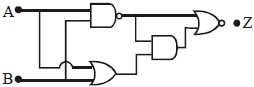
A
$1, 0, 1, 1$
B
$0, 1, 0, 0$
C
$0, 0, 1, 0$
D
$1, 1, 0, 1$
Solution
(C) Let the output of the $NAND$ gate be $P = \overline{AB}$.
Let the output of the $OR$ gate be $Q = A+B$.
The $AND$ gate takes $P$ and $Q$ as inputs,so its output is $R = P \cdot Q = (\overline{AB}) \cdot (A+B)$.
Using Boolean algebra: $R = (\bar{A} + \bar{B}) \cdot (A+B) = \bar{A}A + \bar{A}B + \bar{B}A + \bar{B}B = 0 + \bar{A}B + A\bar{B} + 0 = A \oplus B$ ($XOR$ operation).
The final $NOR$ gate takes $P$ and $R$ as inputs,so $Z = \overline{P+R} = \overline{(\overline{AB}) + (A \oplus B)}$.
Let's evaluate for each input $(A, B)$:
$1$. $(1, 0): P = \overline{1 \cdot 0} = 1, Q = 1+0 = 1, R = 1 \cdot 1 = 1. Z = \overline{1+1} = 0$.
$2$. $(0, 0): P = \overline{0 \cdot 0} = 1, Q = 0+0 = 0, R = 1 \cdot 0 = 0. Z = \overline{1+0} = 0$.
$3$. $(1, 1): P = \overline{1 \cdot 1} = 0, Q = 1+1 = 1, R = 0 \cdot 1 = 0. Z = \overline{0+0} = 1$.
$4$. $(0, 1): P = \overline{0 \cdot 1} = 1, Q = 0+1 = 1, R = 1 \cdot 1 = 1. Z = \overline{1+1} = 0$.
The outputs are $0, 0, 1, 0$.
0 likes
View Solution245
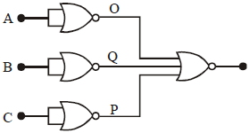
MediumMCQ
Identify the operation performed by the circuit given below.
A
$AND$
B
$NAND$
C
$OR$
D
$NOT$
Solution
(A) The circuit consists of three $NOT$ gates (implemented using $NOR$ gates with shorted inputs) followed by a $NOR$ gate.
Let the inputs be $A, B, C$.
The outputs of the three $NOT$ gates are $A' = \bar{A}$,$B' = \bar{B}$,and $C' = \bar{C}$.
These are fed into a $NOR$ gate. The final output $Y$ is given by:
$Y = \overline{A' + B' + C'} = \overline{\bar{A} + \bar{B} + \bar{C}}$.
Using De Morgan's theorem,$\overline{\bar{A} + \bar{B} + \bar{C}} = \overline{\bar{A}} \cdot \overline{\bar{B}} \cdot \overline{\bar{C}} = A \cdot B \cdot C$.
Thus,the circuit performs the $AND$ operation.
0 likes
View Solution246
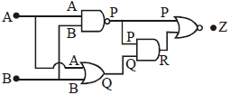
DifficultMCQ
Identify the correct output signal $Y$ in the given combination of gates (as shown) for the given inputs $A$ and $B$.
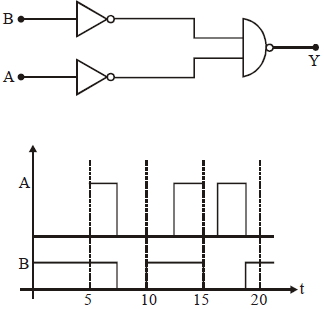
A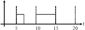
B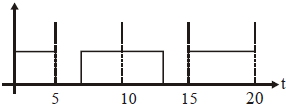
C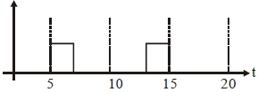
D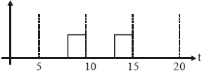
Solution
(B) The given circuit consists of two $NOT$ gates followed by a $NAND$ gate.
The inputs to the $NAND$ gate are $\bar{A}$ and $\bar{B}$.
The output $Y$ of the $NAND$ gate is given by the Boolean expression:
$Y = \overline{\bar{A} \cdot \bar{B}}$
Using De Morgan's theorem,$\overline{X \cdot Y} = \bar{X} + \bar{Y}$.
Therefore,$Y = \overline{\bar{A}} + \overline{\bar{B}} = A + B$.
This represents an $OR$ gate operation.
By analyzing the input waveforms for $A$ and $B$ at different time intervals,we can determine the output $Y = A + B$:
- For $t < 5$,$A=0, B=1 \implies Y=1$.
- For $5 < t < 7$,$A=1, B=1 \implies Y=1$.
- For $7 < t < 10$,$A=0, B=0 \implies Y=0$.
- For $10 < t < 15$,$A=1, B=1 \implies Y=1$.
- For $15 < t < 17$,$A=0, B=0 \implies Y=0$.
- For $17 < t < 19$,$A=1, B=0 \implies Y=1$.
- For $t > 19$,$A=0, B=1 \implies Y=1$.
Comparing this with the given options,the waveform corresponding to the $OR$ operation is represented by option $B$.
0 likes
View Solution247
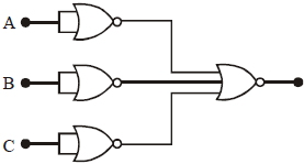
MediumMCQ
For the logic circuit shown,the truth table is:
A
| $A$ | $B$ | $Y$ |
|---|---|---|
| $0$ | $0$ | $1$ |
| $0$ | $1$ | $0$ |
| $1$ | $0$ | $0$ |
| $1$ | $1$ | $0$ |
B
| $A$ | $B$ | $Y$ |
|---|---|---|
| $0$ | $0$ | $0$ |
| $0$ | $1$ | $0$ |
| $1$ | $0$ | $0$ |
| $1$ | $1$ | $1$ |
C
| $A$ | $B$ | $Y$ |
|---|---|---|
| $0$ | $0$ | $0$ |
| $0$ | $1$ | $1$ |
| $1$ | $0$ | $1$ |
| $1$ | $1$ | $1$ |
D
| $A$ | $B$ | $Y$ |
|---|---|---|
| $0$ | $0$ | $1$ |
| $0$ | $1$ | $1$ |
| $1$ | $0$ | $1$ |
| $1$ | $1$ | $0$ |
Solution
(B) The given circuit consists of two $NOT$ gates followed by a $NOR$ gate.
Let the inputs be $A$ and $B$.
The outputs of the two $NOT$ gates are $\bar{A}$ and $\bar{B}$.
These are the inputs to the $NOR$ gate.
The output $Y$ of the $NOR$ gate is given by the Boolean expression:
$Y = \overline{\bar{A} + \bar{B}}$
Using De Morgan's theorem,$\overline{\bar{A} + \bar{B}} = \overline{\bar{A}} \cdot \overline{\bar{B}} = A \cdot B$.
Thus,the circuit acts as an $AND$ gate.
The truth table for an $AND$ gate is:
Therefore,the correct option is $B$.
Let the inputs be $A$ and $B$.
The outputs of the two $NOT$ gates are $\bar{A}$ and $\bar{B}$.
These are the inputs to the $NOR$ gate.
The output $Y$ of the $NOR$ gate is given by the Boolean expression:
$Y = \overline{\bar{A} + \bar{B}}$
Using De Morgan's theorem,$\overline{\bar{A} + \bar{B}} = \overline{\bar{A}} \cdot \overline{\bar{B}} = A \cdot B$.
Thus,the circuit acts as an $AND$ gate.
The truth table for an $AND$ gate is:
| $A$ | $B$ | $Y$ |
|---|---|---|
| $0$ | $0$ | $0$ |
| $0$ | $1$ | $0$ |
| $1$ | $0$ | $0$ |
| $1$ | $1$ | $1$ |
Therefore,the correct option is $B$.
0 likes
View SolutionSemiconductor Electronics — Boolean Algebra and Logic Gates · Frequently Asked Questions
1Are these Semiconductor Electronics questions useful for JEE and NEET?
Yes. All questions in this section are mapped to JEE Main and NEET exam patterns. Previous year questions from JEE Main, NEET, GUJCET and state-level exams are included with full solutions.
2Can I switch to Hindi or Gujarati for these questions?
Yes. Use the language tabs in the hero section or the sidebar to view the same questions and solutions in English, Hindi or Gujarati.
3How do I generate a question paper from this subtopic?
Use the Vedclass Exam Paper Generator — select the chapter and subtopic, set difficulty, and generate Sets A, B, C, D automatically. First 3 chapters of every subject are free.
Vedclass Products
For Students
Vedclass Test Series
Mock tests in real JEE/NEET style with performance analysis. 5-day free trial.
Start Free TrialFor Teachers
Exam Paper Generator
Generate Set A/B/C/D papers from this chapter in 2 minutes. 3 chapters free.
Try FreeFor Institutes
Online Exam Module
Live online exams with unlimited students, 360° analytics & white-label branding.
See DemoFor Teachers & Institutes
Generate a Semiconductor Electronics Exam Paper in 2 Minutes
Select subtopic & difficulty — Sets A, B, C, D auto-generated with No Repeat logic.
First 3 chapters of every subject are free — no payment required.