
A English
PN Junction and Diode Questions in English
Class 12 Physics · Semiconductor Electronics · PN Junction and Diode
404+
Questions
English
Language
100%
With Solutions
Showing 50 of 404 questions in English
51
EasyMCQ
When no bias is applied to a $P-N$ junction,the current is:
A
Zero because the number of charge carriers flowing on both sides is the same.
B
Zero because the charge carriers do not move.
C
Non-zero.
D
None of these.
Solution
(A) In an unbiased $P-N$ junction,a depletion region is formed at the junction interface. This region creates a potential barrier that prevents the net flow of charge carriers across the junction. Although individual charge carriers are in thermal motion,the number of electrons diffusing from the $N$-side to the $P$-side is exactly balanced by the number of electrons drifting from the $P$-side to the $N$-side (and similarly for holes). Therefore,the net current across the junction is zero.
0 likes
View Solution52
EasyMCQ
To make a $PN$ junction conducting,
A
The value of forward bias should be more than the barrier potential.
B
The value of forward bias should be less than the barrier potential.
C
The value of reverse bias should be more than the barrier potential.
D
The value of reverse bias should be less than the barrier potential.
Solution
(A) $PN$ junction diode acts as a conductor when it is forward-biased.
In forward bias,the positive terminal of the battery is connected to the $P$-region and the negative terminal to the $N$-region.
This reduces the width of the depletion layer and the height of the potential barrier.
For significant current to flow,the applied forward bias voltage must exceed the barrier potential (which is approximately $0.7 \ V$ for Silicon and $0.3 \ V$ for Germanium).
Therefore,the correct condition is that the forward bias should be greater than the barrier potential.
0 likes
View Solution53
EasyMCQ
Which is the wrong statement in the following sentences? $A$ device in which $P$ and $N$-type semiconductors are used is more useful than a vacuum tube because:
A
Power is not necessary to heat the filament
B
It is more stable
C
Very less heat is produced in it
D
Its efficiency is high due to a high voltage across the junction
Solution
(D) The correct answer is $D$. In a semiconductor device (like a $PN$ junction diode),the voltage drop across the junction is very low (typically $0.3 \ V$ to $0.7 \ V$). Therefore,the statement that efficiency is high due to a high voltage across the junction is incorrect.
0 likes
View Solution54
EasyMCQ
The depletion layer in a silicon diode is $1 \, \mu m$ wide and the knee potential is $0.6 \, V$. The electric field in the depletion layer is:
A
$Zero$
B
$0.6 \, Vm^{-1}$
C
$6 \times 10^{4} \, V/m$
D
$6 \times 10^{5} \, V/m$
Solution
(D) The electric field $E$ in the depletion layer is given by the formula $E = \frac{V}{d}$, where $V$ is the potential difference (knee potential) and $d$ is the width of the depletion layer.
Given:
Potential $V = 0.6 \, V$
Width $d = 1 \, \mu m = 1 \times 10^{-6} \, m$
Substituting the values:
$E = \frac{0.6 \, V}{1 \times 10^{-6} \, m} = 0.6 \times 10^{6} \, V/m = 6 \times 10^{5} \, V/m$.
Therefore, the correct option is $D$.
Given:
Potential $V = 0.6 \, V$
Width $d = 1 \, \mu m = 1 \times 10^{-6} \, m$
Substituting the values:
$E = \frac{0.6 \, V}{1 \times 10^{-6} \, m} = 0.6 \times 10^{6} \, V/m = 6 \times 10^{5} \, V/m$.
Therefore, the correct option is $D$.
0 likes
View Solution55
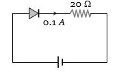
MediumMCQ
$A$ diode having a potential difference of $0.5\, V$ across its junction,which does not depend on the current,is connected in series with a resistance of $20\, \Omega$ across a source. If $0.1\, A$ passes through the resistance,then what is the voltage of the source (in $, V$)?
A
$1.5$
B
$2$
C
$2.5$
D
$5$
Solution
(C) The diode and the resistor are connected in series with the voltage source.
According to Kirchhoff's Voltage Law,the total source voltage $V$ is the sum of the potential difference across the diode $(V_d)$ and the potential difference across the resistor $(V_r)$.
Given:
Potential difference across the diode,$V_d = 0.5\, V$
Resistance,$R = 20\, \Omega$
Current,$I = 0.1\, A$
The potential difference across the resistor is $V_r = I \times R = 0.1\, A \times 20\, \Omega = 2\, V$.
Therefore,the total source voltage is $V = V_d + V_r = 0.5\, V + 2\, V = 2.5\, V$.
0 likes
View Solution56
EasyMCQ
In an experiment,the saturation in the plate current in a diode is observed at $240\,V$. But a student still wants to increase the plate current. It can be done,if
A
The plate voltage is increased further
B
The plate voltage is decreased
C
The filament current is decreased
D
The filament current is increased
Solution
(D) In a diode,saturation current occurs when all the electrons emitted by the filament reach the plate.
Once saturation is reached,increasing the plate voltage further does not increase the plate current because there are no additional electrons available to be collected.
To increase the plate current beyond the saturation point,one must increase the number of electrons emitted per second by the filament.
This is achieved by increasing the temperature of the filament,which is done by increasing the filament current.
Therefore,the correct option is $D$.
0 likes
View Solution57
DifficultMCQ
In a $PN$-junction diode,the reverse saturation current is ${10^{-5}} \ A$ at $27^\circ C$. Calculate the forward current for a voltage of $0.2 \ V$. Given: $[\exp(7.62) = 2038.6, \ k_B = 1.4 \times {10^{-23}} \ J/K, \ e = 1.6 \times {10^{-19}} \ C]$.
A
$2037.6 \times {10^{-3}} \ A$
B
$203.76 \times {10^{-3}} \ A$
C
$20.376 \times {10^{-3}} \ A$
D
$2.0376 \times {10^3} \ A$
Solution
(C) The formula for the forward current $I$ in a $PN$-junction diode is given by $I = I_s (e^{\frac{eV}{k_B T}} - 1)$.
Given:
Reverse saturation current $I_s = {10^{-5}} \ A$
Voltage $V = 0.2 \ V$
Temperature $T = 27^\circ C = 27 + 273 = 300 \ K$
Boltzmann constant $k_B = 1.4 \times {10^{-23}} \ J/K$
Elementary charge $e = 1.6 \times {10^{-19}} \ C$
Exponent value $\frac{eV}{k_B T} = \frac{1.6 \times {10^{-19}} \times 0.2}{1.4 \times {10^{-23}} \times 300} = \frac{0.32 \times {10^{-19}}}{4.2 \times {10^{-21}}} = \frac{32}{4.2} \approx 7.62$.
Substituting the values into the equation:
$I = {10^{-5}} \times (e^{7.62} - 1)$
$I = {10^{-5}} \times (2038.6 - 1)$
$I = {10^{-5}} \times 2037.6$
$I = 20.376 \times {10^{-3}} \ A$.
0 likes
View Solution58
MediumMCQ
$A$ $2V$ battery is connected across the points $A$ and $B$ as shown in the figure. Assuming that the resistance of each diode is zero in forward bias and infinity in reverse bias,the current supplied by the battery when its positive terminal is connected to $A$ is........$A$
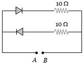
A
$0.2$
B
$0.4$
C
$0$
D
$0.1$
Solution
(A) When the positive terminal of the $2V$ battery is connected to point $A$,the upper diode is forward-biased,while the lower diode is reverse-biased.
In forward bias,the diode acts as a short circuit (resistance = $0 \Omega$).
In reverse bias,the diode acts as an open circuit (resistance = $\infty \Omega$).
Therefore,the current flows only through the upper branch containing the $10 \Omega$ resistor.
The total resistance of the circuit is $R = 10 \Omega$.
The current $I$ supplied by the battery is given by Ohm's law: $I = \frac{V}{R}$.
Substituting the values: $I = \frac{2V}{10 \Omega} = 0.2A$.
0 likes
View Solution59
MediumMCQ
The current $i$ in the circuit will be:
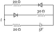
A
$\frac{5}{40} \text{ A}$
B
$\frac{5}{50} \text{ A}$
C
$\frac{5}{10} \text{ A}$
D
$\frac{5}{20} \text{ A}$
Solution
(B) In the given circuit,the battery of $5 \text{ V}$ is connected in series with a $20 \text{ } \Omega$ resistor and two parallel branches.
The upper branch contains a $20 \text{ } \Omega$ resistor and a diode. The diode is connected such that its p-side is towards the right,making it reverse-biased with respect to the positive terminal of the battery.
The middle branch contains a diode and a $30 \text{ } \Omega$ resistor. The diode is connected such that its p-side is towards the left,making it forward-biased with respect to the positive terminal of the battery.
Since the upper branch is reverse-biased,it acts as an open circuit (no current flows through it).
The total resistance of the circuit is the sum of the $20 \text{ } \Omega$ resistor in the main line and the $30 \text{ } \Omega$ resistor in the active middle branch: $R_{eq} = 20 \text{ } \Omega + 30 \text{ } \Omega = 50 \text{ } \Omega$.
Using Ohm's law,the current $i$ is:
$i = \frac{V}{R_{eq}} = \frac{5 \text{ V}}{50 \text{ } \Omega} = \frac{5}{50} \text{ A}$.
0 likes
View Solution60
MediumMCQ
The diode used in the circuit shown in the figure has a constant voltage drop of $0.5\; V$ at all currents and a maximum power rating of $100\; mW$. What should be the value of the resistor $R$,connected in series with the diode,to obtain the maximum current? (in $\Omega$)
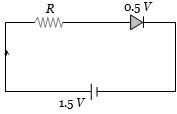
A
$1.5$
B
$5$
C
$6.67$
D
$200$
Solution
(B) The maximum current $I$ that the diode can handle is determined by its maximum power rating $P$ and its constant voltage drop $V_d$.
Given $P = 100\; mW = 100 \times 10^{-3}\; W$ and $V_d = 0.5\; V$.
The maximum current is $I = \frac{P}{V_d} = \frac{100 \times 10^{-3}}{0.5} = 0.2\; A$.
Applying Kirchhoff's Voltage Law to the circuit,the voltage across the resistor $R$ is $V_R = V_{source} - V_d = 1.5\; V - 0.5\; V = 1.0\; V$.
Using Ohm's law,$V_R = I \times R$,so $R = \frac{V_R}{I} = \frac{1.0}{0.2} = 5\; \Omega$.
0 likes
View Solution61
MediumMCQ
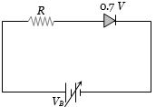
The junction diode in the following circuit requires a minimum current of $1 \, mA$ to be above the knee point $(0.7 \, V)$ of its $I-V$ characteristic curve. The voltage across the diode is independent of current above the knee point. If $V_B = 5 \, V$,then the maximum value of $R$ so that the voltage is above the knee point will be:
A
$4.3 \, k\Omega$
B
$860 \, k\Omega$
C
$4.3 \, \Omega$
D
$860 \, \Omega$
Solution
(A) At the knee point,the voltage across the diode is $V_D = 0.7 \, V$.
Applying Kirchhoff's Voltage Law $(KVL)$ to the circuit,we have $V_B = I \cdot R + V_D$.
Given $V_B = 5 \, V$,$V_D = 0.7 \, V$,and the minimum current $I = 1 \, mA = 1 \times 10^{-3} \, A$.
The voltage across the resistor $R$ is $V_R = V_B - V_D = 5 \, V - 0.7 \, V = 4.3 \, V$.
Using Ohm's law,$V_R = I \cdot R$,we get $4.3 \, V = (1 \times 10^{-3} \, A) \cdot R$.
Therefore,$R = \frac{4.3}{1 \times 10^{-3}} \, \Omega = 4300 \, \Omega = 4.3 \, k\Omega$.
Thus,the maximum value of $R$ is $4.3 \, k\Omega$.
0 likes
View Solution62
DifficultMCQ
In the following circuit,$PN$-junction diodes $D_1$,$D_2$,and $D_3$ are ideal. For the following potentials of $A$ and $B$,the correct increasing order of equivalent resistance between $A$ and $B$ will be:
$(i) V_A = -10 V, V_B = -5 V$
$(ii) V_A = -5 V, V_B = -10 V$
$(iii) V_A = -4 V, V_B = -12 V$
$(i) V_A = -10 V, V_B = -5 V$
$(ii) V_A = -5 V, V_B = -10 V$
$(iii) V_A = -4 V, V_B = -12 V$
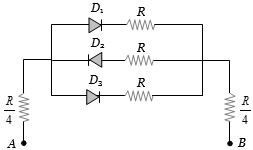
A
$(i) < (ii) < (iii)$
B
$(iii) < (ii) < (i)$
C
$(ii) = (iii) < (i)$
D
$(i) = (iii) < (ii)$
Solution
(C) The circuit consists of three parallel branches,each containing a diode in series with a resistor $R$. The entire combination is in series with two resistors of $R/4$ at terminals $A$ and $B$.
$(i)$ $V_A = -10 V, V_B = -5 V$: Here,$V_A < V_B$. The potential at the anode of $D_2$ is higher than its cathode,making $D_2$ forward-biased. $D_1$ and $D_3$ are reverse-biased. The equivalent resistance is $R_{eq} = R/4 + R + R/4 = 1.5 R$.
$(ii)$ $V_A = -5 V, V_B = -10 V$: Here,$V_A > V_B$. The potential at the anodes of $D_1$ and $D_3$ is higher than their cathodes,making them forward-biased. $D_2$ is reverse-biased. The equivalent resistance is $R_{eq} = R/4 + (R || R) + R/4 = R/4 + R/2 + R/4 = R$.
$(iii)$ $V_A = -4 V, V_B = -12 V$: Here,$V_A > V_B$. Similar to case $(ii)$,$D_1$ and $D_3$ are forward-biased,and $D_2$ is reverse-biased. The equivalent resistance is $R_{eq} = R/4 + (R || R) + R/4 = R$.
Comparing the values: $1.5 R > R$. Thus,$(ii) = (iii) < (i)$.
0 likes
View Solution63
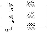
MediumMCQ
The circuit shown in the following figure contains two diodes $D_1$ and $D_2$,each with a forward resistance of $50 \, \Omega$ and infinite backward resistance. If the battery voltage is $6 \, V$,the current through the $100 \, \Omega$ resistance (in amperes) is:
A
$0$
B
$0.02$
C
$0.03$
D
$0.036$
Solution
(B) $1$. Analyze the biasing of the diodes: Based on the provided circuit diagram,the positive terminal of the $6 \, V$ battery is connected to the anode of diode $D_1$ and the cathode of diode $D_2$.
$2$. Determine the state of each diode: Diode $D_1$ is forward-biased,allowing current to flow through it. Diode $D_2$ is reverse-biased,acting as an open circuit (infinite resistance),so no current flows through the branch containing $D_2$.
$3$. Calculate the total resistance of the circuit: The circuit effectively consists of the battery,the $100 \, \Omega$ resistor,the forward-biased diode $D_1$ (with $50 \, \Omega$ resistance),and the $150 \, \Omega$ resistor in series.
Total resistance $R_{eq} = R_{battery} + R_{D1} + R_{150\Omega} + R_{100\Omega} = 0 + 50 \, \Omega + 150 \, \Omega + 100 \, \Omega = 300 \, \Omega$.
$4$. Calculate the current: Using Ohm's law,$I = \frac{V}{R_{eq}} = \frac{6 \, V}{300 \, \Omega} = 0.02 \, A$.
0 likes
View Solution64
MediumMCQ
In a forward biased $PN$-junction diode,the potential barrier in the depletion region is of the form...
A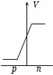
B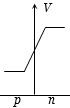
C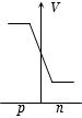
D
Solution
(A) In an unbiased $PN$-junction,there is a potential barrier $V_B$ across the junction,where the $P$-side is at a lower potential and the $N$-side is at a higher potential.
When the diode is forward biased,an external voltage $V$ is applied such that the $P$-side is connected to the positive terminal and the $N$-side is connected to the negative terminal.
This external voltage opposes the built-in potential barrier,effectively reducing the barrier height from $V_B$ to $(V_B - V)$.
The potential profile still shows a transition from a lower potential on the $P$-side to a higher potential on the $N$-side,but the overall height of this step is reduced compared to the unbiased case.
Among the given options,the graph representing a transition from a lower potential on the $P$-side to a higher potential on the $N$-side is shown in option $A$.
0 likes
View Solution65
MediumMCQ
Different voltages are applied across a $P-N$ junction and the currents are measured for each value. Which of the following graphs is obtained between voltage and current?
A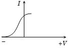
B
C
D
Solution
(B) $P-N$ junction diode exhibits non-linear $V-I$ characteristics.
In forward biasing (positive voltage $+V$),the resistance is very low,allowing a large current to flow,which increases exponentially with voltage.
In reverse biasing (negative voltage $-V$),the resistance is very high,resulting in a negligible (very small) reverse saturation current.
The graph that correctly represents this behavior,showing a sharp increase in current for positive voltage and near-zero current for negative voltage,is represented by the graph in option $B$.
0 likes
View Solution66
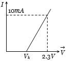
MediumMCQ
The resistance of a germanium junction diode whose $V-I$ characteristic is shown in the figure is ........ $k\Omega$ $(V_k = 0.3 \, V)$.
A
$5$
B
$0.2$
C
$2.3$
D
$\frac{10}{2.3}$
Solution
(B) The resistance of the diode is given by the reciprocal of the slope of the $V-I$ characteristic curve in the forward bias region.
From the graph,the knee voltage $V_k = 0.3 \, V$.
The current $I = 10 \, mA = 10 \times 10^{-3} \, A$ at a voltage $V = 2.3 \, V$.
The dynamic resistance $R$ is calculated as:
$R = \frac{\Delta V}{\Delta I} = \frac{V - V_k}{I - 0}$
$R = \frac{2.3 \, V - 0.3 \, V}{10 \times 10^{-3} \, A - 0}$
$R = \frac{2.0 \, V}{10 \times 10^{-3} \, A} = 0.2 \times 10^3 \, \Omega = 200 \, \Omega$.
Converting to $k\Omega$,we get $R = 0.2 \, k\Omega$.
0 likes
View Solution67
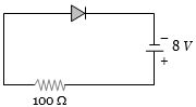
MediumMCQ
$A$ source voltage of $8V$ drives the diode in the figure through a current-limiting resistor of $100 \Omega$. Then the magnitude of the slope of the load line on the $V-I$ characteristics of the diode is
A
$0.01$
B
$100$
C
$0.08$
D
$12.5$
Solution
(A) Let $i$ be the current in the diode and $V$ be the voltage drop across it. According to Kirchhoff's voltage law for the given circuit:
$i \times 100 + V = 8$
Rearranging the equation to express $i$ in terms of $V$:
$i = -\frac{1}{100}V + \frac{8}{100}$
$i = -(0.01)V + 0.08$
Comparing this with the equation of a straight line $y = mx + c$,where $y = i$ and $x = V$,the slope $m$ is given by $-\frac{1}{R}$.
The magnitude of the slope of the load line is $|m| = \frac{1}{R} = \frac{1}{100} = 0.01 \text{ } \Omega^{-1}$.
0 likes
View Solution68
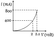
MediumMCQ
The $i-V$ characteristic of a $P-N$ junction diode is shown in the figure. The approximate dynamic resistance of the $P-N$ junction when a forward bias of $2 \; V$ is applied is ....... $\Omega$.
A
$1$
B
$0.25$
C
$0.5$
D
$5$
Solution
(B) The dynamic resistance $R$ is defined as the ratio of the change in voltage to the change in current,given by $R = \frac{\Delta V}{\Delta i}$.
From the given graph,at $V_1 = 2 \; V$,the current is $i_1 = 400 \; mA = 0.4 \; A$.
At $V_2 = 2.1 \; V$,the current is $i_2 = 800 \; mA = 0.8 \; A$.
Calculating the changes:
$\Delta V = V_2 - V_1 = 2.1 \; V - 2.0 \; V = 0.1 \; V$
$\Delta i = i_2 - i_1 = 800 \; mA - 400 \; mA = 400 \; mA = 0.4 \; A$
Therefore,the dynamic resistance is:
$R = \frac{0.1 \; V}{0.4 \; A} = 0.25 \; \Omega$.
Thus,the correct option is $B$.
0 likes
View Solution69
MediumMCQ
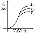
For the diode,the characteristic curves are given at different temperatures. The relation between the temperatures is
A
$T_1 = T_2 = T_3$
B
$T_1 < T_2 < T_3$
C
$T_1 > T_2 > T_3$
D
None of the above
Solution
(B) The characteristic curve of a diode shows the variation of current $(I_p)$ with respect to voltage $(V_p)$ at different temperatures.
As the temperature of a semiconductor diode increases,the number of thermally generated charge carriers increases,which leads to an increase in the saturation current.
From the given graph,for a fixed voltage,the current $I_p$ is highest for $T_3$ and lowest for $T_1$.
Therefore,the relationship between the temperatures is $T_1 < T_2 < T_3$.
0 likes
View Solution70
DifficultMCQ
In a diode $AM$-detector,the output circuit consists of $R = 1 \, k\Omega$ and $C = 10 \, pF$. $A$ carrier signal of $100 \, kHz$ is to be detected. Is it good?
A
Yes
B
No
C
Information is not sufficient
D
None of these
Solution
(B) For proper demodulation in a diode $AM$-detector,the condition $\frac{1}{f_c} \ll RC$ must be satisfied,where $f_c$ is the carrier frequency.
Given:
$f_c = 100 \, kHz = 10^5 \, Hz$
$R = 1 \, k\Omega = 10^3 \, \Omega$
$C = 10 \, pF = 10 \times 10^{-12} \, F = 10^{-11} \, F$
Calculating $\frac{1}{f_c}$:
$\frac{1}{f_c} = \frac{1}{10^5} = 10^{-5} \, s$
Calculating $RC$:
$RC = 10^3 \times 10^{-11} = 10^{-8} \, s$
Comparing the values:
We observe that $10^{-5} \, s > 10^{-8} \, s$,which means $\frac{1}{f_c} > RC$.
Since the condition $\frac{1}{f_c} \ll RC$ is not satisfied,the circuit is not good for detection.
0 likes
View Solution71
EasyMCQ
When a $P-N$ junction is in reverse bias,the current flowing through the junction is primarily due to:
A
Diffusion of charge carriers
B
Deformation of material
C
Drift of charge carriers
D
Both drift and diffusion
Solution
(C) In a $P-N$ junction,when it is reverse biased,the potential barrier at the junction increases.
This prevents the majority charge carriers (holes in $P$-region and electrons in $N$-region) from crossing the junction,effectively stopping the diffusion current.
However,the minority charge carriers (electrons in $P$-region and holes in $N$-region) are pushed across the junction by the electric field created by the reverse bias voltage.
This movement of minority charge carriers is known as drift current.
Therefore,the small reverse saturation current is primarily due to the drift of minority charge carriers.
0 likes
View Solution72
EasyMCQ
The characteristic graph of a diode at different temperatures is shown. What is the relationship between the temperatures?
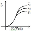
A
None of these.
B
$T_1 < T_2 < T_3$
C
$T_1 > T_2 > T_3$
D
$T_1 = T_2 = T_3$
Solution
(B) For a $PN$ junction diode,the forward current increases with an increase in temperature for a fixed forward voltage.
As the temperature increases,the number of charge carriers increases,leading to a higher current for the same applied voltage.
From the given graph,for a fixed voltage $V_B$,the current $I_p$ is highest for $T_3$ and lowest for $T_1$.
Therefore,the relationship between the temperatures is $T_1 < T_2 < T_3$.
0 likes
View Solution73
EasyMCQ
The depletion layer consists of .......
A
Electrons
B
Holes
C
Mobile ions
D
Immobile ions
Solution
(D) The depletion layer is formed by the diffusion of charge carriers (holes and electrons) across the $p-n$ junction.
When electrons from the $n$-region diffuse into the $p$-region and holes from the $p$-region diffuse into the $n$-region,they recombine near the junction.
This recombination leaves behind ionized donor atoms in the $n$-side (which become positively charged) and ionized acceptor atoms in the $p$-side (which become negatively charged).
These ionized atoms are fixed in the crystal lattice and cannot move; therefore,they are called immobile ions.
Thus,the depletion region is characterized by the presence of these immobile ions,creating an electric field that prevents further diffusion.
Therefore,option $D$ is the correct answer.
0 likes
View Solution74
EasyMCQ
In a $P-N$ junction,when the current value increases,the contact potential ..........
A
increases
B
decreases
C
remains unchanged
D
depends on temperature
Solution
(C) The contact potential (or barrier potential) $V_B$ of a $P-N$ junction is an intrinsic property determined by the doping concentration and the material properties of the semiconductor.
When an external forward bias is applied to the $P-N$ junction,the effective barrier potential decreases,allowing current to flow.
However,the contact potential itself is a fixed characteristic of the junction at a given temperature.
Even when the current increases due to an increase in the applied forward bias,the contact potential (the potential barrier height) remains unchanged as a physical property of the junction structure itself,although the effective barrier height is modified by the external voltage.
0 likes
View Solution75
EasyMCQ
$A$ $P-N$ junction is formed using $Si$ material. What is the approximate height of the depletion barrier in $V$?
A
$1$
B
$10$
C
$0.7$
D
$0.3$
Solution
(C) The potential barrier (or depletion barrier) for a $P-N$ junction depends on the semiconductor material used.
For Silicon $(Si)$,the energy gap is approximately $1.1 \ eV$,and the potential barrier height is typically around $0.7 \ V$ at room temperature.
For Germanium $(Ge)$,the potential barrier height is typically around $0.3 \ V$.
Therefore,for a $Si$ $P-N$ junction,the correct value is $0.7 \ V$.
For Silicon $(Si)$,the energy gap is approximately $1.1 \ eV$,and the potential barrier height is typically around $0.7 \ V$ at room temperature.
For Germanium $(Ge)$,the potential barrier height is typically around $0.3 \ V$.
Therefore,for a $Si$ $P-N$ junction,the correct value is $0.7 \ V$.
0 likes
View Solution76
MediumMCQ
On which of the following does the barrier potential of a $P-N$ junction diode $NOT$ depend?
A
Diode design
B
Temperature
C
Forward bias
D
Doping concentration
Solution
(A) The barrier potential $(V_B)$ of a $P-N$ junction diode is primarily determined by the material properties (like the band gap of the semiconductor) and the doping concentration.
$1$. It depends on the temperature: As temperature increases, the barrier potential decreases.
$2$. It depends on the doping concentration: Higher doping levels generally lead to a higher barrier potential.
$3$. It is affected by the applied forward bias: The effective barrier potential is reduced by the applied forward bias voltage $(V_B - V_{\text{applied}})$.
$4$. Diode design (such as the physical shape or size of the diode) does not affect the intrinsic barrier potential of the $P-N$ junction itself.
Therefore, the barrier potential does not depend on the diode design.
0 likes
View Solution77
MediumMCQ
Application of a forward bias to a $P-N$ junction
A
decreases the electric field in the depletion zone.
B
increases the potential difference across the depletion zone.
C
increases the number of donors on the $N$ side.
D
widens the depletion zone.
Solution
(A) When a $P-N$ junction is forward biased,the positive terminal of the external battery is connected to the $P$-side and the negative terminal to the $N$-side.
This setup opposes the internal electric field of the depletion region.
As a result,the potential barrier height decreases,and the width of the depletion zone decreases.
Since the electric field $E$ is related to the potential barrier $V_B$ and width $W$ by $E = V_B / W$,the reduction in the potential barrier and the narrowing of the depletion region lead to a decrease in the electric field within the depletion zone.
0 likes
View Solution78
MediumMCQ
Which of the following graphs is correct for a $P-N$ junction? (When the $P-N$ junction is forward biased.)
A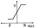
B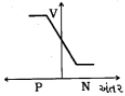
C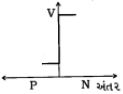
D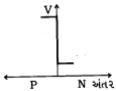
Solution
(B) In a $P-N$ junction,there is a built-in potential barrier at the junction due to the diffusion of charge carriers.
For a $P-N$ junction,the potential on the $P$-side is higher than the potential on the $N$-side in equilibrium.
When the junction is forward biased,the external voltage opposes the built-in potential barrier,reducing the effective barrier height.
However,the potential profile across the junction still shows a decrease from the $P$-side to the $N$-side.
Graph $B$ correctly represents the potential variation across the $P-N$ junction,where the potential is higher on the $P$-side and lower on the $N$-side.
0 likes
View Solution79
MediumMCQ
In a $P-N$ junction,which of the following statements is correct regarding the potential?
A
The potential in the $N$-region is higher than the potential in the $P$-region.
B
The potential in the $P$-region is higher than the potential in the $N$-region.
C
The potential of both the $P$-region and the $N$-region is the same.
D
Nothing can be said.
Solution
(B) When a $P-N$ junction is formed,electrons diffuse from the $N$-region to the $P$-region due to the concentration gradient.
This diffusion leaves behind immobile positive ions in the $N$-region and negative ions in the $P$-region near the junction.
This creates an electric field directed from the $N$-region to the $P$-region.
Consequently,the potential of the $P$-region becomes higher than that of the $N$-region,creating a potential barrier.
0 likes
View Solution80
MediumMCQ
In a forward-biased $P-N$ junction diode,how does the potential barrier behave?
A
B
C
D
Solution
(A) When a $P-N$ junction diode is forward-biased,the positive terminal of the external battery is connected to the $P$-region and the negative terminal to the $N$-region.
This external electric field opposes the internal electric field of the depletion region.
As a result,the width of the depletion layer decreases and the potential barrier height is reduced.
Therefore,the potential barrier height decreases in a forward-biased $P-N$ junction diode.
This external electric field opposes the internal electric field of the depletion region.
As a result,the width of the depletion layer decreases and the potential barrier height is reduced.
Therefore,the potential barrier height decreases in a forward-biased $P-N$ junction diode.
0 likes
View Solution81
EasyMCQ
$P-N$ junction is said to be forward biased,when
A
the positive pole of the battery is joined to the $p$-semiconductor and negative pole to the $n$-semiconductor
B
the positive pole of the battery is joined to the $n$-semiconductor and negative pole to the $p$-semiconductor
C
the positive pole of the battery is connected to $n$-semiconductor and $p$-semiconductor
D
a mechanical force is applied in the forward direction.
Solution
(A) $P-N$ junction is said to be forward biased when the positive terminal of an external battery is connected to the $p$-type semiconductor and the negative terminal is connected to the $n$-type semiconductor.
In this configuration,the potential barrier at the junction is reduced,allowing majority charge carriers (holes in $p$-side and electrons in $n$-side) to cross the junction easily,resulting in a significant current flow.
In this configuration,the potential barrier at the junction is reduced,allowing majority charge carriers (holes in $p$-side and electrons in $n$-side) to cross the junction easily,resulting in a significant current flow.
0 likes
View Solution82
MediumMCQ
Which graph represents the variation of charge density with distance across a $P-N$ junction?
A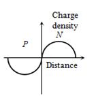
B
C
D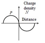
Solution
(A) In a $P-N$ junction,the depletion region is formed by the diffusion of charge carriers.
On the $P$-side of the junction,there are immobile negatively charged acceptor ions.
On the $N$-side of the junction,there are immobile positively charged donor ions.
Therefore,the charge density is negative on the $P$-side and positive on the $N$-side.
Graph $A$ correctly depicts this distribution,where the charge density is negative for $P$ (left of the junction) and positive for $N$ (right of the junction).
0 likes
View Solution83
MediumMCQ
If the forward voltage in a diode is increased,the thickness of the depletion layer .......
A
increases
B
decreases
C
fluctuates
D
remains unchanged
Solution
(B) In a $P-N$ junction diode,when a forward bias voltage is applied,the positive terminal of the battery is connected to the $P$-region and the negative terminal to the $N$-region.
This external electric field opposes the internal electric field of the depletion region.
As the forward voltage increases,the potential barrier decreases,which causes the majority charge carriers (holes in $P$ and electrons in $N$) to be pushed towards the junction.
Consequently,the width of the depletion layer decreases.
0 likes
View Solution84
MediumMCQ
In the figure,two $P-N$ junctions are connected. In which of the following connections will the voltages across the $P-N$ junctions be equal?
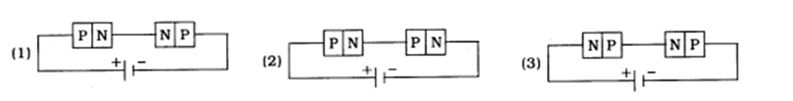
A
$(1)$ and $(2)$
B
Only $(1)$
C
$(2)$ and $(3)$
D
$(1)$ and $(3)$
Solution
(C) In circuit $(1)$,the two diodes are connected in series such that one is forward-biased and the other is reverse-biased. Due to the symmetry of the circuit,the potential drop across each diode is not necessarily equal.
In circuit $(2)$,both diodes are identical and connected in series in the same orientation (both forward-biased). Due to symmetry,the voltage drop across each diode will be equal.
In circuit $(3)$,both diodes are identical and connected in series in the same orientation (both reverse-biased). Due to symmetry,the voltage drop across each diode will be equal.
Therefore,in circuits $(2)$ and $(3)$,the voltages across the $P-N$ junctions are equal due to the identical nature and symmetric configuration of the diodes.
0 likes
View Solution85
EasyMCQ
The width of the depletion layer is approximately .......
A
$0.5$ $\mu$m
B
$0.05$ $\mu$m
C
$0.5$ mm
D
$0.005$ $\mu$m
Solution
(A) In a $P-N$ junction diode,the depletion layer (or depletion region) is formed due to the diffusion of charge carriers across the junction.
This region is characterized by the absence of mobile charge carriers.
The width of this depletion layer is typically in the order of $10^{-6}$ meters,which is equivalent to $1$ $\mu$m.
Specifically,for most standard semiconductor diodes,the width of the depletion layer is approximately $0.5$ $\mu$m.
0 likes
View Solution86
EasyMCQ
$A$ $P-N$ junction is a ............ .
A
Ohmic resistor
B
Non-ohmic resistor
C
Positive resistor
D
Negative resistor
Solution
(B) Ohm's law states that for an ohmic conductor,the current $I$ is directly proportional to the potential difference $V$,resulting in a linear $I-V$ characteristic graph.
In a $P-N$ junction diode,the current $I$ does not vary linearly with the potential difference $V$.
The $I-V$ characteristic curve of a $P-N$ junction diode is non-linear,showing exponential growth in forward bias and negligible current in reverse bias.
Therefore,a $P-N$ junction diode does not follow Ohm's law and is classified as a non-ohmic device.
0 likes
View Solution87
EasyMCQ
In a $P-N$ junction under reverse bias,the depletion layer contains .......
A
Zero electric field
B
Maximum electric potential
C
Maximum electric field
D
Zero electric potential
Solution
(C) When a $P-N$ junction is reverse biased,the external voltage is applied in the same direction as the built-in potential barrier.
This causes the depletion region to widen.
Since the number of charge carriers (holes in $P$-side and electrons in $N$-side) is pushed away from the junction,the depletion layer consists of immobile ionized atoms.
The electric field in the depletion region increases significantly because the potential barrier height increases,leading to a maximum electric field at the junction interface.
0 likes
View Solution88
MediumMCQ
When a $P-N$ junction is forward biased,which of the following is true?
A
The positive terminal of the battery is connected to the $P$-region of the $P-N$ junction,and the depletion region is wide.
B
The positive terminal of the battery is connected to the $N$-region of the $P-N$ junction,and the depletion layer is wide.
C
The positive terminal of the battery is connected to the $N$-region of the junction,and the depletion region is thin.
D
The positive terminal of the battery is connected to the $P$-region of the junction,and the depletion region is thin.
Solution
(D) In a $P-N$ junction,forward biasing occurs when the positive terminal of the external battery is connected to the $P$-type semiconductor and the negative terminal is connected to the $N$-type semiconductor.
In this configuration,the holes in the $P$-region are pushed towards the junction,and the electrons in the $N$-region are pushed towards the junction.
This action reduces the width of the depletion layer and lowers the potential barrier,allowing current to flow easily across the junction.
Therefore,the positive terminal is connected to the $P$-region,and the depletion region becomes thin.
0 likes
View Solution89
EasyMCQ
The $P-N$ junction depletion layer is made up of .......
A
Only electrons
B
Electrons and holes
C
Only holes
D
Neither holes nor electrons
Solution
(D) When $p$-type and $n$-type semiconductors are joined,the electrons in the $n$-type region diffuse into the $p$-type region across the junction,whereas holes in the $p$-type region diffuse into the $n$-type region across the junction.
This diffusion process leaves behind immobile ionized impurity atoms (positive ions on the $n$-side and negative ions on the $p$-side) near the junction.
Because these ions are fixed in the crystal lattice and cannot move,the depletion region is essentially devoid of mobile charge carriers (free electrons and holes).
Therefore,the depletion layer consists of immobile ions,and it contains neither free electrons nor free holes.
0 likes
View Solution90
EasyMCQ
$A$ device is connected to a supply such that one end is connected to the positive terminal and the other to the negative terminal. If the connections are reversed and no current flows,the device is a .......
A
$P-N$ junction diode
B
Transistor
C
Zener diode
D
Triode
Solution
(A) $P-N$ junction diode allows current to flow when it is forward-biased (positive terminal to $P$-side,negative terminal to $N$-side).
When the connections are reversed,the diode is reverse-biased.
In reverse bias,the depletion layer widens,offering very high resistance,and practically no current flows through the circuit.
Therefore,the device described is a $P-N$ junction diode.
When the connections are reversed,the diode is reverse-biased.
In reverse bias,the depletion layer widens,offering very high resistance,and practically no current flows through the circuit.
Therefore,the device described is a $P-N$ junction diode.
0 likes
View Solution91
EasyMCQ
What is the cause of the formation of the depletion layer in a $P-N$ junction?
A
Due to the drift of holes
B
Due to the diffusion of charge carriers
C
Due to the movement of impurity ions
D
Due to the drift of electrons
Solution
(B) When a $P-N$ junction is formed,the difference in concentration of charge carriers between the $P$ and $N$ regions leads to the diffusion of electrons from the $N$-side to the $P$-side and holes from the $P$-side to the $N$-side.
As these charge carriers cross the junction,they recombine near the interface.
This recombination leaves behind immobile ionized impurity atoms (negative ions on the $P$-side and positive ions on the $N$-side).
These immobile ions create an electric field that opposes further diffusion,resulting in a region depleted of mobile charge carriers,known as the depletion layer.
Therefore,the depletion region is primarily caused by the diffusion of charge carriers.
0 likes
View Solution92
EasyMCQ
When a $P-N$ junction is reverse biased,then ...
A
The barrier potential decreases.
B
The barrier potential increases.
C
The number of majority charge carriers increases.
D
The number of minority charge carriers increases.
Solution
(B) In a reverse bias condition,the external battery potential and the depletion layer potential are in the same direction,which opposes the flow of majority charge carriers.
As a result,the width of the depletion region increases,and the barrier potential increases.
As a result,the width of the depletion region increases,and the barrier potential increases.
0 likes
View Solution93
MediumMCQ
When a $P-N$ junction is in forward bias,what happens to the depletion region and the potential barrier?
A
The depletion region decreases and the potential barrier height increases.
B
The depletion region widens and the potential barrier height decreases.
C
Both the depletion region and the potential barrier height decrease.
D
Both the depletion region and the potential barrier height increase.
Solution
(C) In a $P-N$ junction,when forward bias is applied,the positive terminal of the battery is connected to the $P$-region and the negative terminal to the $N$-region.
This external electric field opposes the internal electric field of the depletion region.
As a result,the majority charge carriers are pushed towards the junction,which reduces the width of the depletion region.
Since the depletion region width decreases,the potential barrier height also decreases,making it easier for charge carriers to cross the junction.
0 likes
View Solution94
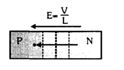
MediumMCQ
$A$ $P-N$ junction has a potential barrier of $0.5 \ V$. If the depletion region is $5 \times 10^{-7} \ m$ wide,what will be the intensity of the electric field in this region?
A
$10^3 \ V/m$
B
$10^2 \ V/m$
C
$10^6 \ V/m$
D
$10^8 \ V/m$
Solution
(C) The potential barrier $V = 0.5 \ V$.
The width of the depletion region $\Delta L = 5 \times 10^{-7} \ m$.
The electric field intensity $E$ is given by the formula:
$E = \frac{V}{\Delta L}$
Substituting the given values:
$E = \frac{0.5 \ V}{5 \times 10^{-7} \ m} = \frac{0.5}{5} \times 10^7 \ V/m = 0.1 \times 10^7 \ V/m = 10^6 \ V/m$.
The width of the depletion region $\Delta L = 5 \times 10^{-7} \ m$.
The electric field intensity $E$ is given by the formula:
$E = \frac{V}{\Delta L}$
Substituting the given values:
$E = \frac{0.5 \ V}{5 \times 10^{-7} \ m} = \frac{0.5}{5} \times 10^7 \ V/m = 0.1 \times 10^7 \ V/m = 10^6 \ V/m$.
1 likes
View Solution95
EasyMCQ
Which of the following options is correct for the $P-N$ junction diode shown in the figure?
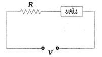
A
When the diode is forward-biased,the voltage across the resistor $R$ will be $V$.
B
When the diode is reverse-biased,the voltage across the resistor $R$ will be $V$.
C
In forward-biased condition,the voltage across the resistor $R$ will be $2V$.
D
In reverse-biased condition,the voltage across the resistor $R$ will be $2V$.
Solution
(A) An ideal $P-N$ junction diode acts as a closed switch (zero resistance) when forward-biased. In this state,the entire voltage $V$ of the source appears across the resistor $R$.
When the diode is reverse-biased,it acts as an open switch (infinite resistance). In this state,no current flows through the circuit,and the voltage drop across the resistor $R$ is $0 \ V$.
When the diode is reverse-biased,it acts as an open switch (infinite resistance). In this state,no current flows through the circuit,and the voltage drop across the resistor $R$ is $0 \ V$.
0 likes
View Solution96
MediumMCQ
The ratio of the resistance of a $P-N$ junction diode in forward bias to its resistance in reverse bias is approximately:
A
$10^2:1$
B
$10^{-2}:1$
C
$1:10^{-4}$
D
$1:10^4$
Solution
(D) In a $P-N$ junction diode,the forward bias resistance $(R_f)$ is typically in the range of $10 \ \Omega$ to $100 \ \Omega$.
The reverse bias resistance $(R_r)$ is typically in the range of $10^5 \ \Omega$ to $10^6 \ \Omega$.
Therefore,the ratio of forward bias resistance to reverse bias resistance is given by:
$\frac{R_f}{R_r} \approx \frac{10^1}{10^5} = 10^{-4}$ or $1:10^4$.
Thus,the ratio is $1:10^4$.
The reverse bias resistance $(R_r)$ is typically in the range of $10^5 \ \Omega$ to $10^6 \ \Omega$.
Therefore,the ratio of forward bias resistance to reverse bias resistance is given by:
$\frac{R_f}{R_r} \approx \frac{10^1}{10^5} = 10^{-4}$ or $1:10^4$.
Thus,the ratio is $1:10^4$.
0 likes
View Solution97
MediumMCQ
If the voltage across the diode in the given circuit is $0.5 \ V$,then the current flowing through the circuit is ...... $mA$.
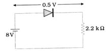
A
$3.4$
B
$2$
C
$2.5$
D
$3$
Solution
(A) Applying Kirchhoff's voltage law to the circuit:
$8 \ V - 0.5 \ V - I \times (2.2 \ k\Omega) = 0$
$8 - 0.5 = I \times (2.2 \times 10^3 \ \Omega)$
$7.5 = I \times 2200 \ \Omega$
$I = \frac{7.5}{2200} \ A$
$I = 0.003409 \ A \approx 3.41 \times 10^{-3} \ A$
$I \approx 3.4 \ mA$
$8 \ V - 0.5 \ V - I \times (2.2 \ k\Omega) = 0$
$8 - 0.5 = I \times (2.2 \times 10^3 \ \Omega)$
$7.5 = I \times 2200 \ \Omega$
$I = \frac{7.5}{2200} \ A$
$I = 0.003409 \ A \approx 3.41 \times 10^{-3} \ A$
$I \approx 3.4 \ mA$
0 likes
View Solution98
MediumMCQ
In a semiconductor diode,the forward voltage is increased from $0.5 \ V$ to $0.7 \ V$. As a result,the forward current changes by $1 \ mA$. The forward resistance of the diode is ....... $\Omega$.
A
$100$
B
$120$
C
$200$
D
$240$
Solution
(C) The change in forward voltage is $\Delta V = 0.7 \ V - 0.5 \ V = 0.2 \ V$.
The change in forward current is $\Delta I = 1 \ mA = 10^{-3} \ A$.
The forward resistance of the diode is given by the formula $r_{fb} = \frac{\Delta V}{\Delta I}$.
Substituting the values,we get $r_{fb} = \frac{0.2}{10^{-3}} = 200 \ \Omega$.
The change in forward current is $\Delta I = 1 \ mA = 10^{-3} \ A$.
The forward resistance of the diode is given by the formula $r_{fb} = \frac{\Delta V}{\Delta I}$.
Substituting the values,we get $r_{fb} = \frac{0.2}{10^{-3}} = 200 \ \Omega$.
0 likes
View Solution99
MediumMCQ
The $I-V$ characteristic of a $P-N$ junction diode is shown in the figure. The approximate dynamic resistance of the $P-N$ junction when a forward bias of $1\;V$ is applied is.......$\Omega$.
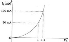
A
$2$
B
$0.2$
C
$20$
D
$0.5$
Solution
(A) The dynamic resistance $r_f$ of a $P-N$ junction diode is defined as the ratio of the change in voltage to the change in current in the forward bias region.
$r_f = \frac{\Delta V_f}{\Delta I_f}$
From the given graph,at $V_f = 1\;V$,$I_f = 50\;mA$ and at $V_f = 1.1\;V$,$I_f = 100\;mA$.
Therefore,$\Delta V_f = 1.1\;V - 1.0\;V = 0.1\;V$.
And $\Delta I_f = 100\;mA - 50\;mA = 50\;mA = 50 \times 10^{-3}\;A$.
Now,substituting these values into the formula:
$r_f = \frac{0.1}{50 \times 10^{-3}} = \frac{0.1 \times 1000}{50} = \frac{100}{50} = 2\;\Omega$.
Thus,the approximate dynamic resistance is $2\;\Omega$.
0 likes
View Solution100
MediumMCQ
In the given figure,a $Si$ diode and a $Ge$ diode are connected in series. What should be the potential at point $A$ to bring both diodes into forward bias?
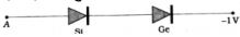
A
$0 \ V$
B
$-2 \ V$
C
$+0.7 \ V$
D
$+0.3 \ V$
Solution
(A) For a $Si$ diode,the barrier potential is approximately $0.7 \ V$,and for a $Ge$ diode,it is approximately $0.3 \ V$.
Since the diodes are in series,the total potential drop required to forward bias both is $V_{total} = 0.7 \ V + 0.3 \ V = 1.0 \ V$.
The cathode of the $Ge$ diode is connected to a potential of $-1 \ V$.
Let the potential at point $A$ be $V_A$.
For the diodes to be in forward bias,the potential difference across the series combination must be at least $1.0 \ V$.
Thus,$V_A - (-1 \ V) = 1.0 \ V$.
$V_A + 1 \ V = 1.0 \ V$.
$V_A = 0 \ V$.
0 likes
View SolutionSemiconductor Electronics — PN Junction and Diode · Frequently Asked Questions
1Are these Semiconductor Electronics questions useful for JEE and NEET?
Yes. All questions in this section are mapped to JEE Main and NEET exam patterns. Previous year questions from JEE Main, NEET, GUJCET and state-level exams are included with full solutions.
2Can I switch to Hindi or Gujarati for these questions?
Yes. Use the language tabs in the hero section or the sidebar to view the same questions and solutions in English, Hindi or Gujarati.
3How do I generate a question paper from this subtopic?
Use the Vedclass Exam Paper Generator — select the chapter and subtopic, set difficulty, and generate Sets A, B, C, D automatically. First 3 chapters of every subject are free.
Vedclass Products
For Students
Vedclass Test Series
Mock tests in real JEE/NEET style with performance analysis. 5-day free trial.
Start Free TrialFor Teachers
Exam Paper Generator
Generate Set A/B/C/D papers from this chapter in 2 minutes. 3 chapters free.
Try FreeFor Institutes
Online Exam Module
Live online exams with unlimited students, 360° analytics & white-label branding.
See DemoFor Teachers & Institutes
Generate a Semiconductor Electronics Exam Paper in 2 Minutes
Select subtopic & difficulty — Sets A, B, C, D auto-generated with No Repeat logic.
First 3 chapters of every subject are free — no payment required.