
A English
Boolean Algebra and Logic Gates Questions in English
Class 12 Physics · Semiconductor Electronics · Boolean Algebra and Logic Gates
483+
Questions
English
Language
100%
With Solutions
Showing 50 of 483 questions in English
101
MediumMCQ
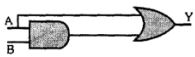
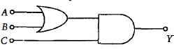
What is the truth table for the given logic gate combination?
A
| $A$ | $B$ | $Y$ |
| $0$ | $0$ | $0$ |
| $0$ | $1$ | $0$ |
| $1$ | $0$ | $1$ |
| $1$ | $1$ | $1$ |
B
| $A$ | $B$ | $Y$ |
| $0$ | $0$ | $0$ |
| $0$ | $1$ | $0$ |
| $1$ | $0$ | $0$ |
| $1$ | $1$ | $1$ |
C
| $A$ | $B$ | $Y$ |
| $0$ | $0$ | $1$ |
| $0$ | $1$ | $1$ |
| $1$ | $0$ | $1$ |
| $1$ | $1$ | $0$ |
D
| $A$ | $B$ | $Y$ |
| $0$ | $0$ | $0$ |
| $0$ | $1$ | $1$ |
| $1$ | $0$ | $1$ |
| $1$ | $1$ | $0$ |
Solution
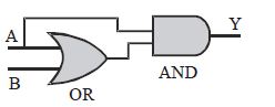
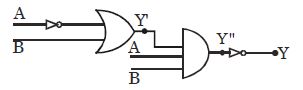
(A) The given circuit consists of an $AND$ gate and an $OR$ gate.
Let the inputs be $A$ and $B$.
The output of the $AND$ gate is $A \cdot B$.
This output is one of the inputs to the $OR$ gate,while the other input to the $OR$ gate is $A$ directly.
Therefore,the final output $Y$ is given by the Boolean expression: $Y = A + (A \cdot B)$.
Using the Boolean algebra identity $A + (A \cdot B) = A(1 + B) = A \cdot 1 = A$,we find that $Y = A$.
Let's verify this with a truth table:
- If $A=0, B=0$: $Y = 0 + (0 \cdot 0) = 0 + 0 = 0$.
- If $A=0, B=1$: $Y = 0 + (0 \cdot 1) = 0 + 0 = 0$.
- If $A=1, B=0$: $Y = 1 + (1 \cdot 0) = 1 + 0 = 1$.
- If $A=1, B=1$: $Y = 1 + (1 \cdot 1) = 1 + 1 = 1$.
Comparing this with the given options,option $A$ matches this truth table.
0 likes
View Solution102
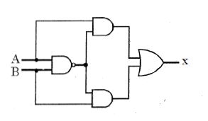
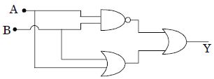
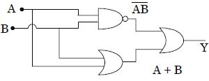
MediumMCQ
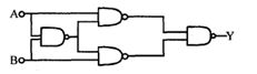
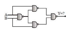
The truth table for the given circuit of four $NAND$ gates is:
A
| $A$ | $B$ | $Y$ |
| $0$ | $0$ | $1$ |
| $0$ | $1$ | $0$ |
| $1$ | $0$ | $0$ |
| $1$ | $1$ | $1$ |
B
| $A$ | $B$ | $Y$ |
| $0$ | $0$ | $0$ |
| $0$ | $1$ | $1$ |
| $1$ | $0$ | $1$ |
| $1$ | $1$ | $0$ |
C
| $A$ | $B$ | $Y$ |
| $0$ | $0$ | $0$ |
| $0$ | $1$ | $0$ |
| $1$ | $0$ | $1$ |
| $1$ | $1$ | $1$ |
D
| $A$ | $B$ | $Y$ |
| $0$ | $0$ | $1$ |
| $0$ | $1$ | $1$ |
| $1$ | $0$ | $0$ |
| $1$ | $1$ | $0$ |
Solution
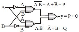
(B) Let the inputs be $A$ and $B$.
$1$. The first $NAND$ gate produces output $C = \overline{A \cdot B}$.
$2$. The second $NAND$ gate (top) takes inputs $A$ and $C$, producing $D = \overline{A \cdot C} = \overline{A \cdot (\overline{A \cdot B})} = \overline{A \cdot (\overline{A} + \overline{B})} = \overline{A \cdot \overline{A} + A \cdot \overline{B}} = \overline{0 + A \cdot \overline{B}} = \overline{A \cdot \overline{B}} = \overline{A} + B$.
$3$. The third $NAND$ gate (bottom) takes inputs $B$ and $C$, producing $E = \overline{B \cdot C} = \overline{B \cdot (\overline{A \cdot B})} = \overline{B \cdot (\overline{A} + \overline{B})} = \overline{B \cdot \overline{A} + B \cdot \overline{B}} = \overline{B \cdot \overline{A} + 0} = \overline{B \cdot \overline{A}} = \overline{B} + A$.
$4$. The final $NAND$ gate takes inputs $D$ and $E$, producing $Y = \overline{D \cdot E} = \overline{(\overline{A} + B) \cdot (A + \overline{B})} = \overline{\overline{A} \cdot A + \overline{A} \cdot \overline{B} + B \cdot A + B \cdot \overline{B}} = \overline{0 + \overline{A} \cdot \overline{B} + A \cdot B + 0} = \overline{\overline{A} \cdot \overline{B} + A \cdot B} = A \oplus B$ ($XOR$ gate).
The correct table is $B$.
0 likes
View Solution103
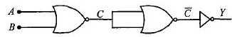
DifficultMCQ
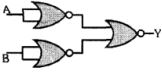
What logic gate is formed by the combination of gates shown below?
A
$OR$ gate
B
$AND$ gate
C
$NOR$ gate
D
$NAND$ gate
Solution
(B) The given circuit consists of two $NOT$ gates (formed by shorting the inputs of two $NOR$ gates) followed by a $NOR$ gate.
Let the inputs be $A$ and $B$.
The output of the first $NOR$ gate with inputs $A$ and $A$ is $Y_1 = \overline{A+A} = \overline{A}$.
The output of the second $NOR$ gate with inputs $B$ and $B$ is $Y_2 = \overline{B+B} = \overline{B}$.
These outputs $Y_1$ and $Y_2$ are fed into the final $NOR$ gate.
The final output $Y$ is given by $Y = \overline{Y_1 + Y_2} = \overline{\overline{A} + \overline{B}}$.
Using De Morgan's theorem,$\overline{\overline{A} + \overline{B}} = \overline{\overline{A}} \cdot \overline{\overline{B}} = A \cdot B$.
Thus,the final output is $Y = A \cdot B$,which represents an $AND$ gate.
0 likes
View Solution104
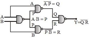
DifficultMCQ
What will be the outputs $Y$ for the inputs $(A = 1, B = 0)$,$(A = 1, B = 1)$,and $(A = 0, B = 0)$ respectively?
A
$0, 1, 1$
B
$0, 0, 1$
C
$1, 1, 1$
D
$1, 0, 0$
Solution
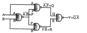
(D) Let the output of the first $NAND$ gate be $P = \overline{A \cdot B}$.
The inputs to the top $NAND$ gate are $A$ and $P$,so its output is $Q = \overline{A \cdot P} = \overline{A \cdot \overline{A \cdot B}} = \overline{A} + (A \cdot B) = \overline{A} + B$.
The inputs to the bottom $NAND$ gate are $P$ and $B$,so its output is $R = \overline{P \cdot B} = \overline{\overline{A \cdot B} \cdot B} = (A \cdot B) + \overline{B} = A + \overline{B}$.
The final output $Y$ is the output of the last $NAND$ gate with inputs $Q$ and $R$:
$Y = \overline{Q \cdot R} = \overline{Q} + \overline{R} = \overline{\overline{A} + B} + \overline{A + \overline{B}} = (A \cdot \overline{B}) + (\overline{A} \cdot B)$.
This is the expression for an $XOR$ gate.
$1$. For $(A = 1, B = 0)$: $Y = (1 \cdot \overline{0}) + (\overline{1} \cdot 0) = (1 \cdot 1) + (0 \cdot 0) = 1 + 0 = 1$.
$2$. For $(A = 1, B = 1)$: $Y = (1 \cdot \overline{1}) + (\overline{1} \cdot 1) = (1 \cdot 0) + (0 \cdot 1) = 0 + 0 = 0$.
$3$. For $(A = 0, B = 0)$: $Y = (0 \cdot \overline{0}) + (\overline{0} \cdot 0) = (0 \cdot 1) + (1 \cdot 0) = 0 + 0 = 0$.
Thus,the outputs are $1, 0, 0$.
0 likes
View Solution105
DifficultMCQ
Identify the logic gate represented by the given circuit.
A
$OR$
B
$AND$
C
$NOR$
D
$XOR$
Solution
(A) The circuit consists of two $NAND$ gates. The top $NAND$ gate has inputs $A$ and $A$ (implied by the connection), but looking at the diagram, the top gate has input $A$ and the bottom gate has input $B$. Wait, let's re-examine the diagram: The top gate has input $A$ (connected to both terminals), acting as a $NOT$ gate. The bottom gate has input $B$ (connected to both terminals), also acting as a $NOT$ gate. The outputs of these two $NOT$ gates are fed into a third $NAND$ gate.
Let the output of the top $NAND$ gate be $Y_1 = \overline{A \cdot A} = \overline{A}$.
Let the output of the bottom $NAND$ gate be $Y_2 = \overline{B \cdot B} = \overline{B}$.
The final output $C$ is the $NAND$ of $Y_1$ and $Y_2$:
$C = \overline{Y_1 \cdot Y_2} = \overline{\overline{A} \cdot \overline{B}}$.
Using De Morgan's theorem, $\overline{\overline{A} \cdot \overline{B}} = \overline{\overline{A}} + \overline{\overline{B}} = A + B$.
Thus, the circuit represents an $OR$ gate.
0 likes
View Solution106
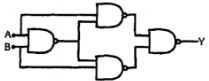
MediumMCQ
Identify the logic gate represented by the given circuit.
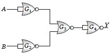
A
$AND$
B
$XOR$
C
$NOR$
D
$NAND$
Solution
(D) The circuit consists of four $NOR$ gates $(G_1, G_2, G_3, G_4)$.
$G_1$ and $G_2$ act as $NOT$ gates because their inputs are tied together. Thus,the outputs are $\bar{A}$ and $\bar{B}$ respectively.
These are fed into $G_3$,which is a $NOR$ gate. Its output is $\overline{\bar{A} + \bar{B}} = \overline{\bar{A}} \cdot \overline{\bar{B}} = A \cdot B$ (by De Morgan's Law).
This output is fed into $G_4$,which acts as a $NOT$ gate. Its output is $\overline{A \cdot B}$.
Thus,the final output $Y = \overline{A \cdot B}$,which is the Boolean expression for a $NAND$ gate.
0 likes
View Solution107
MediumMCQ
What is the output $D$ for the inputs $(A=0, B=0, C=0)$ and $(A=1, B=1, C=0)$ respectively?
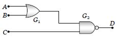
A
$0, 0$
B
$0, 1$
C
$1, 0$
D
$1, 1$
Solution
(D) The circuit consists of an $OR$ gate $(G_1)$ followed by a $NAND$ gate $(G_2)$.
Let the output of the $OR$ gate be $Y$. Then $Y = A + B$.
The final output $D$ is the output of the $NAND$ gate, which is $D = \overline{Y \cdot C} = \overline{(A + B) \cdot C}$.
Case $1$: $A=0, B=0, C=0$.
$Y = 0 + 0 = 0$.
$D = \overline{0 \cdot 0} = \overline{0} = 1$.
Case $2$: $A=1, B=1, C=0$.
$Y = 1 + 1 = 1$.
$D = \overline{1 \cdot 0} = \overline{0} = 1$.
Thus, the outputs are $1, 1$.
0 likes
View Solution108
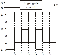
MediumMCQ
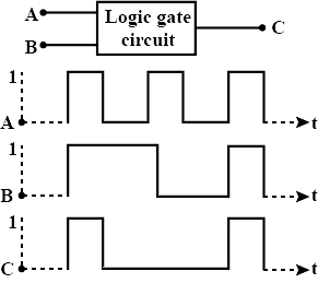
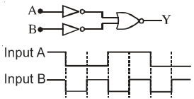
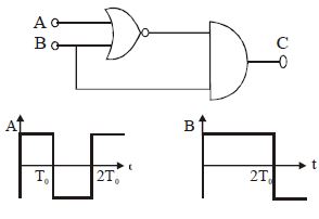
The following figure shows a logic gate circuit with two inputs $A$ and $B$ and the output $C$. The voltage waveforms of $A$,$B$,and $C$ are as shown below. The logic circuit gate is
A
$OR$ gate
B
$AND$ gate
C
$NAND$ gate
D
$NOR$ gate
Solution
(B) By observing the given voltage waveforms,we can construct the truth table for the inputs $A$ and $B$ and the output $C$:
Comparing this truth table with the standard truth tables of logic gates,we find that the output $C$ is $1$ only when both inputs $A$ and $B$ are $1$. This is the characteristic behavior of an $AND$ gate. Therefore,the logic circuit gate is an $AND$ gate.
| $A$ | $B$ | $C$ |
|---|---|---|
| $1$ | $1$ | $1$ |
| $1$ | $0$ | $0$ |
| $0$ | $1$ | $0$ |
| $0$ | $0$ | $0$ |
Comparing this truth table with the standard truth tables of logic gates,we find that the output $C$ is $1$ only when both inputs $A$ and $B$ are $1$. This is the characteristic behavior of an $AND$ gate. Therefore,the logic circuit gate is an $AND$ gate.
0 likes
View Solution109
MediumMCQ
In the following circuit,the output $Y$ for all possible inputs $A$ and $B$ is expressed by the truth table.
A
| $A, B, Y$ |
| $0, 0, 1$ |
| $0, 1, 1$ |
| $1, 0, 1$ |
| $1, 1, 0$ |
B
| $A, B, Y$ |
| $0, 0, 1$ |
| $0, 1, 0$ |
| $1, 0, 0$ |
| $1, 1, 0$ |
C
| $A, B, Y$ |
| $0, 0, 0$ |
| $0, 1, 1$ |
| $1, 0, 1$ |
| $1, 1, 1$ |
D
| $A, B, Y$ |
| $0, 0, 0$ |
| $0, 1, 0$ |
| $1, 0, 0$ |
| $1, 1, 1$ |
Solution
(C) The circuit consists of a $NOR$ gate followed by a $NOR$ gate acting as a $NOT$ gate (since both inputs are tied together).
Let the output of the first $NOR$ gate be $Y^{\prime} = \overline{A + B}$.
The second gate is a $NOR$ gate with both inputs as $Y^{\prime}$,so its output is $Y = \overline{Y^{\prime} + Y^{\prime}} = \overline{Y^{\prime}} = \overline{\overline{A + B}} = A + B$.
This is the Boolean expression for an $OR$ gate.
The truth table for $Y = A + B$ is:
Comparing this with the given options,option $C$ is correct.
Let the output of the first $NOR$ gate be $Y^{\prime} = \overline{A + B}$.
The second gate is a $NOR$ gate with both inputs as $Y^{\prime}$,so its output is $Y = \overline{Y^{\prime} + Y^{\prime}} = \overline{Y^{\prime}} = \overline{\overline{A + B}} = A + B$.
This is the Boolean expression for an $OR$ gate.
The truth table for $Y = A + B$ is:
| $A$ | $B$ | $Y$ |
| $0$ | $0$ | $0$ |
| $0$ | $1$ | $1$ |
| $1$ | $0$ | $1$ |
| $1$ | $1$ | $1$ |
Comparing this with the given options,option $C$ is correct.
0 likes
View Solution110
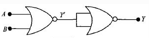
MediumMCQ
The given logic circuit is equivalent to which of the following gates?
A
$NOR$ gate
B
$OR$ gate
C
$AND$ gate
D
$NAND$ gate
Solution
(A) Let the inputs be $A$ and $B$.
$1$. The first gate is a $NOR$ gate,so its output is $X = \overline{A+B}$.
$2$. The second gate is a $NAND$ gate with both inputs tied together. $A$ $NAND$ gate with tied inputs acts as a $NOT$ gate. Thus,the output of the $NAND$ gate is $Z = \overline{X \cdot X} = \overline{X}$.
$3$. Substituting $X = \overline{A+B}$ into $Z$,we get $Z = \overline{\overline{A+B}} = A+B$.
$4$. The third gate is a $NOT$ gate,so its final output is $Y = \overline{Z} = \overline{A+B}$.
$5$. The expression $\overline{A+B}$ represents a $NOR$ gate.
Therefore,the circuit is equivalent to a $NOR$ gate.
0 likes
View Solution111
MediumMCQ
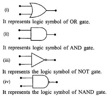
The symbolic representations of four logic gates are given below. The logic symbols for $OR$,$NOT$,and $NAND$ gates are respectively:
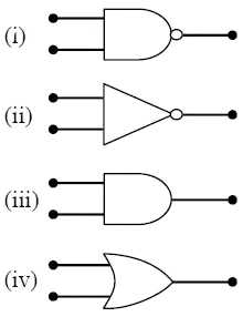
A
$iv, ii$ and $i$
B
$iv, i$ and $iii$
C
$i, iii$ and $iv$
D
$iii, iv$ and $ii$
Solution
(A) By observing the given logic gate symbols:
$(i)$ represents a $NAND$ gate.
(ii) represents a $NOT$ gate.
(iii) represents an $AND$ gate.
(iv) represents an $OR$ gate.
Therefore,the symbols for $OR$,$NOT$,and $NAND$ gates are $(iv)$,$(ii)$,and $(i)$ respectively.
$(i)$ represents a $NAND$ gate.
(ii) represents a $NOT$ gate.
(iii) represents an $AND$ gate.
(iv) represents an $OR$ gate.
Therefore,the symbols for $OR$,$NOT$,and $NAND$ gates are $(iv)$,$(ii)$,and $(i)$ respectively.
0 likes
View Solution112
MediumMCQ
The following figure shows a logic gate circuit with two inputs $A$ and $B$ and the output $Y.$ The voltage waveforms of $A, B$ and $Y$ are as given. The logic gate is
A
$NOR$ gate
B
$OR$ gate
C
$AND$ gate
D
$NAND$ gate
Solution
(D) By observing the given voltage waveforms,we can construct the truth table for the logic gate:
From the truth table,it is clear that the output $Y$ is $0$ only when both inputs $A$ and $B$ are $1.$ In all other cases,the output is $1.$ This behavior corresponds to the $NAND$ gate.
| $A$ | $B$ | $Y$ |
| $1$ | $1$ | $0$ |
| $0$ | $0$ | $1$ |
| $0$ | $1$ | $1$ |
| $1$ | $0$ | $1$ |
From the truth table,it is clear that the output $Y$ is $0$ only when both inputs $A$ and $B$ are $1.$ In all other cases,the output is $1.$ This behavior corresponds to the $NAND$ gate.
0 likes
View Solution113
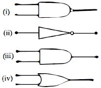
EasyMCQ
The symbolic representations of four logic gates are shown below. Identify which ones correspond to $AND$,$NAND$,and $NOT$ gates,respectively.
A
$(ii), (iii)$ and $(iv)$
B
$(iii), (ii)$ and $(i)$
C
$(iii), (i)$ and $(iv)$
D
$(ii), (iv)$ and $(iii)$
Solution
(D) Based on the standard logic gate symbols:
$(i)$ represents an $OR$ gate.
(ii) represents an $AND$ gate.
(iii) represents a $NOT$ gate (specifically,a $NOT$ gate with two inputs is often represented as a $NOR$ or $NAND$ variant,but in this context,it is identified as a $NOT$ gate symbol).
(iv) represents a $NAND$ gate.
Therefore,the sequence for $AND, NAND$,and $NOT$ gates is $(ii), (iv)$,and $(iii)$ respectively.
0 likes
View Solution114
MediumMCQ
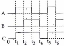
The figure shows a logic circuit with two inputs $A$ and $B$ and the output $C.$ The voltage waveforms across $A, B$ and $C$ are as given. The logic circuit gate is
A
$OR$ gate
B
$NAND$ gate
C
$NOR$ gate
D
$AND$ gate
Solution
(A) To identify the logic gate,we analyze the truth table from the given waveforms:
Comparing this with the truth tables of standard gates:
- For an $OR$ gate,the output is $1$ if at least one input is $1$.
- The observed output $C$ follows the condition: $C = 1$ if $A=1$ or $B=1$,and $C = 0$ if $A=0$ and $B=0$.
- This corresponds exactly to the truth table of an $OR$ gate.
| Time Interval | Input $A$ | Input $B$ | Output $C$ |
|---|---|---|---|
| $0$ to $t_1$ | $0$ | $0$ | $0$ |
| $t_1$ to $t_2$ | $1$ | $0$ | $1$ |
| $t_2$ to $t_3$ | $1$ | $1$ | $1$ |
| $t_3$ to $t_4$ | $0$ | $1$ | $1$ |
| $t_4$ to $t_5$ | $0$ | $0$ | $0$ |
| $t_5$ to $t_6$ | $1$ | $0$ | $1$ |
Comparing this with the truth tables of standard gates:
- For an $OR$ gate,the output is $1$ if at least one input is $1$.
- The observed output $C$ follows the condition: $C = 1$ if $A=1$ or $B=1$,and $C = 0$ if $A=0$ and $B=0$.
- This corresponds exactly to the truth table of an $OR$ gate.
0 likes
View Solution115
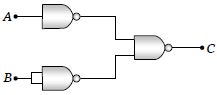
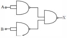
EasyMCQ
The output $(X)$ of the logic circuit shown in the figure will be:
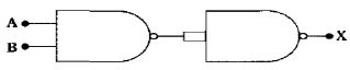
A
$X = A + B$
B
$X = \overline{A.B}$
C
$X = A.B$
D
$X = \overline{A+B}$
Solution
(C) The first gate is a $NAND$ gate with inputs $A$ and $B$. Its output is $\overline{A.B}$.
This output is fed into a $NOT$ gate (a $NAND$ gate with both inputs connected together acts as a $NOT$ gate).
If the input to a $NOT$ gate is $Y$,the output is $\overline{Y}$.
Here,$Y = \overline{A.B}$,so the final output $X = \overline{\overline{A.B}}$.
Using the Boolean algebra property $\overline{\overline{Z}} = Z$,we get $X = A.B$.
0 likes
View Solution116
MediumMCQ
To get output $Y=1$ for the following circuit,the inputs should be:
A
$A=1, B=0, C=0$
B
$A=1, B=1, C=0$
C
$A=1, B=0, C=1$
D
$A=0, B=1, C=0$
Solution
(C) The given circuit consists of an $OR$ gate followed by an $AND$ gate.
Let the output of the $OR$ gate be $X$. Then $X = A + B$.
The final output $Y$ is the output of the $AND$ gate,which takes $X$ and $C$ as inputs.
Therefore,$Y = X \cdot C = (A + B) \cdot C$.
For the output $Y$ to be $1$,both inputs to the $AND$ gate must be $1$.
This means $X = 1$ and $C = 1$.
Since $X = A + B$,for $X$ to be $1$,at least one of $A$ or $B$ must be $1$.
Checking the options:
Option $A$: $A=1, B=0, C=0 \implies Y = (1+0) \cdot 0 = 0$.
Option $B$: $A=1, B=1, C=0 \implies Y = (1+1) \cdot 0 = 0$.
Option $C$: $A=1, B=0, C=1 \implies Y = (1+0) \cdot 1 = 1 \cdot 1 = 1$.
Option $D$: $A=0, B=1, C=0 \implies Y = (0+1) \cdot 0 = 0$.
Thus,the correct option is $C$.
0 likes
View Solution117
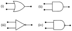
MediumMCQ
From the circuit of the following logic gates,the basic logic gate obtained is
A
B
C
D
Solution
(D) Let the inputs be $A$ and $B$. The outputs of the two $NOT$ gates are $\overline{A}$ and $\overline{B}$.
These are fed into a $NOR$ gate,so the output of the $NOR$ gate is $\overline{\overline{A} + \overline{B}}$.
By De Morgan's theorem,$\overline{\overline{A} + \overline{B}} = \overline{\overline{A}} \cdot \overline{\overline{B}} = A \cdot B$.
This output $(A \cdot B)$ and the input $B$ are fed into a $NAND$ gate.
The final output $Y = \overline{(A \cdot B) \cdot B} = \overline{A \cdot (B \cdot B)}$.
Since $B \cdot B = B$,we have $Y = \overline{A \cdot B}$.
This is the Boolean expression for a $NAND$ gate. However,looking at the provided circuit image,the final gate is a $NAND$ gate,and the expression simplifies to $Y = \overline{A \cdot B}$,which is a $NAND$ gate.
0 likes
View Solution118
MediumMCQ
The given electrical network is equivalent to
A
$AND$ gate
B
$OR$ gate
C
$NOT$ gate
D
$NOR$ gate
Solution
(D) The circuit consists of a $NOR$ gate followed by another $NOR$ gate acting as a $NOT$ gate (both inputs tied together),followed by a $NOT$ gate. Let the output of the first $NOR$ gate be $C = \overline{A+B}$.
This signal $C$ is fed into the second $NOR$ gate,which acts as a $NOT$ gate,producing $\overline{C} = \overline{\overline{A+B}} = A+B$.
Finally,this signal is passed through a $NOT$ gate,giving the final output $Y = \overline{\overline{C}} = \overline{A+B}$.
Thus,the circuit is equivalent to a $NOR$ gate.
0 likes
View Solution119
DifficultMCQ
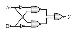
In the combination of the following gates,the output $Y$ can be written in terms of inputs $A$ and $B$ as
A
$\overline {A\cdot B} $
B
$A\cdot \overline {B} + \overline {A} \cdot B$
C
$\overline {A + B}$
D
$\overline {A\cdot B} + A\cdot B$
Solution
(B) The given circuit consists of two $AND$ gates,two $NOT$ gates,and one $OR$ gate.
$1$. The upper $AND$ gate receives inputs $A$ and $\overline{B}$ (since $B$ passes through a $NOT$ gate). Its output is $A \cdot \overline{B}$.
$2$. The lower $AND$ gate receives inputs $\overline{A}$ (since $A$ passes through a $NOT$ gate) and $B$. Its output is $\overline{A} \cdot B$.
$3$. These two outputs are fed into an $OR$ gate. Therefore,the final output $Y$ is the sum of these two expressions: $Y = A \cdot \overline{B} + \overline{A} \cdot B$.
This is the Boolean expression for an $XOR$ (Exclusive-$OR$) gate.
0 likes
View Solution120
MediumMCQ
In the Boolean algebra,$(\overline {\bar A \cdot \bar B} ) \cdot A$ is equal to:
A
$\overline {A + B} $
B
$A$
C
$\overline {A \cdot B} $
D
$A + B$
Solution
(B) Using De Morgan's Law,$\overline {\bar A \cdot \bar B} = \overline{\bar A} + \overline{\bar B} = A + B$.
Substituting this into the expression: $(A + B) \cdot A$.
Expanding the expression: $A \cdot A + B \cdot A$.
Since $A \cdot A = A$,we get $A + AB$.
Factoring out $A$: $A(1 + B)$.
Since $(1 + B) = 1$,the expression simplifies to $A \cdot 1 = A$.
Substituting this into the expression: $(A + B) \cdot A$.
Expanding the expression: $A \cdot A + B \cdot A$.
Since $A \cdot A = A$,we get $A + AB$.
Factoring out $A$: $A(1 + B)$.
Since $(1 + B) = 1$,the expression simplifies to $A \cdot 1 = A$.
0 likes
View Solution121
DifficultMCQ
In the given circuit as shown,two input waveforms $A$ and $B$ are applied simultaneously. The resultant waveform $Y$ is:
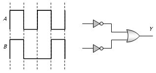
A
B
C
D
Solution
(A) In the given circuit,the inputs $A$ and $B$ are passed through $NOT$ gates before being fed into an $OR$ gate.
Let $A$ and $B$ be the input signals where $1$ represents high and $0$ represents low.
From the waveform,the sequence for $A$ is $1, 0, 1, 0$ and for $B$ is $1, 1, 0, 0$.
After passing through the $NOT$ gates,the inputs to the $OR$ gate become $A' = 0, 1, 0, 1$ and $B' = 0, 0, 1, 1$.
The $OR$ gate performs the operation $Y = A' + B'$.
Calculating the output sequence:
For the first interval: $0 + 0 = 0$
For the second interval: $1 + 0 = 1$
For the third interval: $0 + 1 = 1$
For the fourth interval: $1 + 1 = 1$
Thus,the resultant sequence for $Y$ is $0, 1, 1, 1$. This corresponds to option $A$.
0 likes
View Solution122
MediumMCQ
In the circuit below,$A$ and $B$ represent two inputs and $C$ represents the output.
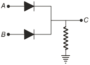
A
$OR$ gate
B
$NOR$ gate
C
$AND$ gate
D
$NAND$ gate
Solution
(A) The given circuit consists of two diodes connected in parallel with a common resistor connected to the ground.
Let us analyze the truth table for this circuit:
$1$. When both inputs $A$ and $B$ are at low potential $(0)$,both diodes are reverse-biased (or non-conducting),so the output $C$ is at ground potential $(0)$.
$2$. When either $A$ or $B$ is at high potential $(1)$,the corresponding diode becomes forward-biased and conducts,pulling the output $C$ to a high potential $(1)$.
$3$. This behavior corresponds to the Boolean expression $C = A + B$,which is the characteristic operation of an $OR$ gate.
Let us analyze the truth table for this circuit:
| $A$ | $B$ | $C$ |
| $0$ | $0$ | $0$ |
| $0$ | $1$ | $1$ |
| $1$ | $0$ | $1$ |
| $1$ | $1$ | $1$ |
$1$. When both inputs $A$ and $B$ are at low potential $(0)$,both diodes are reverse-biased (or non-conducting),so the output $C$ is at ground potential $(0)$.
$2$. When either $A$ or $B$ is at high potential $(1)$,the corresponding diode becomes forward-biased and conducts,pulling the output $C$ to a high potential $(1)$.
$3$. This behavior corresponds to the Boolean expression $C = A + B$,which is the characteristic operation of an $OR$ gate.
0 likes
View Solution123
MediumMCQ
The logic circuit shown below has the input waveforms $A$ and $B$ as shown. Pick out the correct output waveform.
A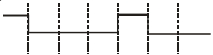
B
C
D
Solution
(D) The given circuit consists of two $NOT$ gates followed by a $NOR$ gate.
Let the inputs be $A$ and $B$. The outputs of the $NOT$ gates are $\bar{A}$ and $\bar{B}$.
These are fed into a $NOR$ gate,so the final output $Y$ is:
$Y = \overline{\bar{A} + \bar{B}}$
Using De Morgan's theorem,$\overline{\bar{A} + \bar{B}} = \overline{\bar{A}} \cdot \overline{\bar{B}} = A \cdot B$.
Thus,the circuit acts as an $AND$ gate.
The truth table for an $AND$ gate is:
Comparing the input waveforms $A$ and $B$ with the $AND$ gate logic,the output $Y$ is high $(1)$ only when both $A$ and $B$ are high $(1)$. Looking at the provided waveforms,this corresponds to option $D$.
Let the inputs be $A$ and $B$. The outputs of the $NOT$ gates are $\bar{A}$ and $\bar{B}$.
These are fed into a $NOR$ gate,so the final output $Y$ is:
$Y = \overline{\bar{A} + \bar{B}}$
Using De Morgan's theorem,$\overline{\bar{A} + \bar{B}} = \overline{\bar{A}} \cdot \overline{\bar{B}} = A \cdot B$.
Thus,the circuit acts as an $AND$ gate.
The truth table for an $AND$ gate is:
| $A$ | $B$ | $Y$ |
| $0$ | $0$ | $0$ |
| $0$ | $1$ | $0$ |
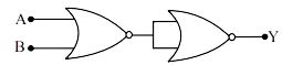
| $1$ | $0$ | $0$ |
| $1$ | $1$ | $1$ |
Comparing the input waveforms $A$ and $B$ with the $AND$ gate logic,the output $Y$ is high $(1)$ only when both $A$ and $B$ are high $(1)$. Looking at the provided waveforms,this corresponds to option $D$.
0 likes
View Solution124
MediumMCQ
The combination of gates shown below yields:
A
$NAND$ gate
B
$OR$ gate
C
$NOT$ gate
D
$XOR$ gate
Solution
(B) The circuit consists of two $NAND$ gates acting as $NOT$ gates (since their inputs are shorted) followed by a $NAND$ gate.
Let the inputs be $A$ and $B$.
The output of the first $NAND$ gate is $\bar{A}$.
The output of the second $NAND$ gate is $\bar{B}$.
These two outputs are fed into the third $NAND$ gate.
The final output $X$ is given by the boolean expression:
$X = \overline{\bar{A} \cdot \bar{B}}$
Using De Morgan's theorem,$\overline{\bar{A} \cdot \bar{B}} = \overline{\bar{A}} + \overline{\bar{B}} = A + B$.
Since the expression $X = A + B$ represents an $OR$ gate,the correct option is $B$.
0 likes
View Solution125
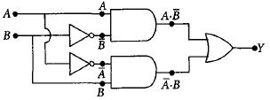
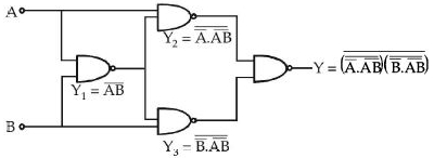
DifficultMCQ
The truth table for the system of four $NAND$ gates as shown in the figure is:
A
| $A$ | $B$ | $Y$ |
| $0$ | $0$ | $1$ |
| $0$ | $1$ | $0$ |
| $1$ | $0$ | $0$ |
| $1$ | $1$ | $0$ |
B
| $A$ | $B$ | $Y$ |
| $0$ | $0$ | $0$ |
| $0$ | $1$ | $1$ |
| $1$ | $0$ | $1$ |
| $1$ | $1$ | $0$ |
C
| $A$ | $B$ | $Y$ |
| $0$ | $0$ | $0$ |
| $0$ | $1$ | $0$ |
| $1$ | $0$ | $1$ |
| $1$ | $1$ | $1$ |
D
| $A$ | $B$ | $Y$ |
| $0$ | $0$ | $1$ |
| $0$ | $1$ | $1$ |
| $1$ | $0$ | $0$ |
| $1$ | $1$ | $0$ |
Solution
(B) Let the output of the first $NAND$ gate be $Y_1 = \overline{A \cdot B}$.
This $Y_1$ is fed into the next two $NAND$ gates.
The output of the second $NAND$ gate is $Y_2 = \overline{A \cdot Y_1} = \overline{A \cdot (\overline{A \cdot B})} = \overline{A} + (A \cdot B) = \overline{A} + B$.
The output of the third $NAND$ gate is $Y_3 = \overline{B \cdot Y_1} = \overline{B \cdot (\overline{A \cdot B})} = \overline{B} + (A \cdot B) = \overline{B} + A$.
The final output $Y$ is the $NAND$ of $Y_2$ and $Y_3$:
$Y = \overline{Y_2 \cdot Y_3} = \overline{(\overline{A} + B) \cdot (\overline{B} + A)} = \overline{(\overline{A} \cdot \overline{B} + \overline{A} \cdot A + B \cdot \overline{B} + B \cdot A)} = \overline{(\overline{A} \cdot \overline{B} + 0 + 0 + A \cdot B)} = \overline{\overline{A} \cdot \overline{B}} + \overline{A \cdot B} = (A + B) \cdot (\overline{A} + \overline{B}) = A \cdot \overline{B} + B \cdot \overline{A}$.
This is the Boolean expression for an $XOR$ gate.
The truth table for an $XOR$ gate is:
If $A=0, B=0$, then $Y=0$.
If $A=0, B=1$, then $Y=1$.
If $A=1, B=0$, then $Y=1$.
If $A=1, B=1$, then $Y=0$.
This matches option $B$.
0 likes
View Solution126
MediumMCQ
If $a, b, c, d$ are inputs to a gate and $x$ is its output,then,as per the following time graph,the gate is
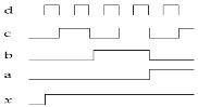
A
$OR$
B
$NAND$
C
$NOT$
D
$AND$
Solution
(A) By observing the time graph,we can analyze the relationship between inputs $a, b, c, d$ and output $x$.
In the given graph,the output $x$ becomes high $(1)$ as soon as any of the inputs $(a, b, c, d)$ becomes high $(1)$.
Specifically,at the beginning,all inputs are $0$ and the output $x$ is $0$.
As soon as the first pulse occurs in input $d$,the output $x$ transitions to $1$ and remains $1$ for the rest of the duration,regardless of the states of other inputs.
This behavior,where the output is $1$ if at least one input is $1$,is the characteristic truth table behavior of an $OR$ gate.
Therefore,the gate is an $OR$ gate.
0 likes
View Solution127
DifficultMCQ
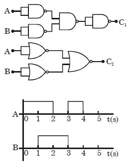
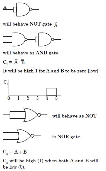
Draw the output signals $C_1$ and $C_2$ for the given combination of logic gates. (Up to $5 \ s$)
A
B
C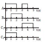
D
Solution
(D) For the first circuit,the input $A$ and $B$ are passed through $NAND$ gates acting as $NOT$ gates,resulting in $\bar{A}$ and $\bar{B}$. These are then fed into a $NAND$ gate,giving $\overline{\bar{A} \cdot \bar{B}} = A + B$. This is then passed through another $NOT$ gate ($NAND$ as $NOT$),resulting in $C_1 = \overline{A + B} = \bar{A} \cdot \bar{B}$. Thus,$C_1$ is high $(1)$ only when both $A$ and $B$ are low $(0)$. Looking at the input graphs,$A=0$ and $B=0$ only in the interval $t = 4 \ s$ to $5 \ s$. Therefore,$C_1$ is high from $4 \ s$ to $5 \ s$.
For the second circuit,the inputs $A$ and $B$ are passed through $NOR$ gates acting as $NOT$ gates,resulting in $\bar{A}$ and $\bar{B}$. These are then fed into a $NOR$ gate,giving $C_2 = \overline{\bar{A} + \bar{B}} = A \cdot B$. Thus,$C_2$ is high $(1)$ only when both $A$ and $B$ are high $(1)$. Looking at the input graphs,$A=1$ and $B=1$ only in the interval $t = 1 \ s$ to $2 \ s$. Therefore,$C_2$ is high from $1 \ s$ to $2 \ s$.
Comparing this with the given options,the correct output signals match option $D$.
0 likes
View Solution128
MediumMCQ
The logic circuit shown has the input waveforms $A$ and $B$ as shown. Pick out the $CORRECT$ output waveform.
A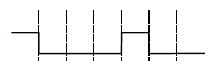
B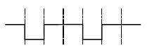
C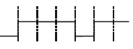
D
Solution
(C) The given circuit consists of two $NOT$ gates at the inputs,followed by a $NOR$ gate,and finally another $NOT$ gate at the output.
Let the inputs be $A$ and $B$.
The outputs of the first two $NOT$ gates are $\bar{A}$ and $\bar{B}$.
These are fed into a $NOR$ gate,so its output is $\overline{\bar{A} + \bar{B}}$.
By De Morgan's Law,$\overline{\bar{A} + \bar{B}} = \overline{\bar{A}} \cdot \overline{\bar{B}} = A \cdot B$.
This output is then passed through a final $NOT$ gate,so the final output $Y = \overline{A \cdot B}$.
This is the Boolean expression for a $NAND$ gate.
$A$ $NAND$ gate gives a low output $(0)$ only when both inputs are high $(1)$. In all other cases,the output is high $(1)$.
Comparing this logic with the given input waveforms,the output waveform corresponds to option $C$.
0 likes
View Solution129
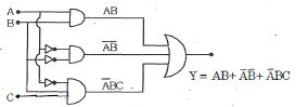
DifficultMCQ
In a digital circuit for three input signals $(A, B, \text{ and } C)$, the final output $(Y)$ should be such that for inputs:
| $A$ | $B$ | $C$ |
|---|---|---|
| $0$ | $0$ | $0$ |
| $0$ | $0$ | $1$ |
| $0$ | $1$ | $0$ |
the output $(Y)$ should be $0$, and for all other cases, it should be $1$. Which of the following digital circuits will give such output?
| $A$ | $B$ | $C$ |
|---|---|---|
| $0$ | $0$ | $0$ |
| $0$ | $0$ | $1$ |
| $0$ | $1$ | $0$ |
the output $(Y)$ should be $0$, and for all other cases, it should be $1$. Which of the following digital circuits will give such output?
A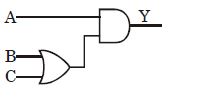
B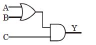
C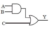
D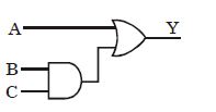
Solution
(D) To find the correct circuit, we analyze the given truth table conditions where $Y = 0$:
$1$. For $(A, B, C) = (0, 0, 0)$, $Y = 0$.
$2$. For $(A, B, C) = (0, 0, 1)$, $Y = 0$.
$3$. For $(A, B, C) = (0, 1, 0)$, $Y = 0$.
Let's evaluate the circuit in option $D$ (image $814-$d281), which consists of an $AND$ gate with inputs $B$ and $C$, followed by an $OR$ gate with inputs $A$ and the output of the $AND$ gate. The Boolean expression is $Y = A + (B \cdot C)$.
Testing the inputs:
- For $(0, 0, 0)$: $Y = 0 + (0 \cdot 0) = 0 + 0 = 0$.
- For $(0, 0, 1)$: $Y = 0 + (0 \cdot 1) = 0 + 0 = 0$.
- For $(0, 1, 0)$: $Y = 0 + (1 \cdot 0) = 0 + 0 = 0$.
- For $(0, 1, 1)$: $Y = 0 + (1 \cdot 1) = 0 + 1 = 1$.
- For $(1, 0, 0)$: $Y = 1 + (0 \cdot 0) = 1 + 0 = 1$.
- For $(1, 0, 1)$: $Y = 1 + (0 \cdot 1) = 1 + 0 = 1$.
- For $(1, 1, 0)$: $Y = 1 + (1 \cdot 0) = 1 + 0 = 1$.
- For $(1, 1, 1)$: $Y = 1 + (1 \cdot 1) = 1 + 1 = 1$.
This matches the required output conditions perfectly. Therefore, the correct circuit is $D$.
0 likes
View Solution130
MediumMCQ
The output $Y$ of the combination of gates shown is equal to :-
A
$A$
B
$\bar A$
C
$A+B$
D
$AB$
Solution
(A) The given circuit consists of an $OR$ gate and an $AND$ gate.
$1$. The inputs to the $OR$ gate are $A$ and $B$. Therefore,the output of the $OR$ gate is $(A + B)$.
$2$. The inputs to the $AND$ gate are $A$ and the output of the $OR$ gate,which is $(A + B)$.
$3$. The output $Y$ of the $AND$ gate is the product of its inputs: $Y = A \cdot (A + B)$.
$4$. Using the Boolean algebra law of absorption,$A \cdot (A + B) = A$.
$5$. Therefore,the final output is $Y = A$.
0 likes
View Solution131
MediumMCQ
Select the outputs $Y$ of the combination of gates shown below for inputs $A = 0, B = 0$; $A = 1, B = 1$ and $A = 0, B = 1$ respectively.
A
$(0, 1, 1)$
B
$(0, 0, 1)$
C
$(1, 0, 0)$
D
$(1, 1, 1)$
Solution
(B) Let the output of the first $NAND$ gate be $P = \overline{A \cdot B}$.
The inputs to the upper $NAND$ gate are $A$ and $P$, so its output is $Q = \overline{A \cdot P}$.
The inputs to the lower $NAND$ gate are $P$ and $B$, so its output is $R = \overline{P \cdot B}$.
The final output $Y$ is the output of a $NAND$ gate with inputs $Q$ and $R$, so $Y = \overline{Q \cdot R}$.
Using De Morgan's Law: $Y = \overline{Q} + \overline{R} = \overline{\overline{A \cdot P}} + \overline{\overline{P \cdot B}} = (A \cdot P) + (P \cdot B) = P \cdot (A + B)$.
Substituting $P = \overline{A \cdot B} = \overline{A} + \overline{B}$, we get $Y = (\overline{A} + \overline{B}) \cdot (A + B) = \overline{A} \cdot B + A \cdot \overline{B}$.
This is the expression for an $XOR$ gate.
For $A = 0, B = 0$: $Y = 0 \oplus 0 = 0$.
For $A = 1, B = 1$: $Y = 1 \oplus 1 = 0$.
For $A = 0, B = 1$: $Y = 0 \oplus 1 = 1$.
Thus, the outputs are $(0, 0, 1)$.
0 likes
View Solution132
DifficultMCQ
The output $y$ of the given logic gate network is:
A
$\bar A.B + A.\bar B$
B
$A.B + \bar A.\bar B$
C
$\left( {\overline {A + B} } \right).\bar A.\bar B$
D
None
Solution
(D) Let the inputs to the two $NAND$ gates be $P$ and $Q$.
From the circuit diagram,the upper $NAND$ gate has inputs $\bar A$ and $B$. Its output is $P = \overline{\bar A \cdot B} = A + \bar B$.
The lower $NAND$ gate has inputs $A$ and $\bar B$. Its output is $Q = \overline{A \cdot \bar B} = \bar A + B$.
The final gate is a $NOR$ gate,so the output $y = \overline{P + Q}$.
Substituting the values of $P$ and $Q$:
$y = \overline{(A + \bar B) + (\bar A + B)}$
$y = \overline{(A + \bar A) + (B + \bar B)}$
Since $A + \bar A = 1$ and $B + \bar B = 1$:
$y = \overline{1 + 1} = \overline{1} = 0$.
Thus,the output $y = 0$.
0 likes
View Solution133
DifficultMCQ
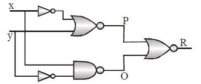
The figure shows a system of logic gates. From the study of the truth table,it can be found that to produce a high output $(1)$ at $R$,we must have
A
$X = 0, Y = 1$
B
$X = 1, Y = 1$
C
$X = 1, Y = 0$
D
Not possible
Solution
(D) Let the inputs be $X$ and $Y$. The top branch consists of a $NOT$ gate followed by a $NOR$ gate. The input to the $NOR$ gate is $\bar{X}$ and $Y$. Thus,$P = \overline{\bar{X} + Y} = X \cdot \bar{Y}$.
The bottom branch consists of a $NAND$ gate with inputs $X$ and $\bar{Y}$. Thus,$Q = \overline{X \cdot \bar{Y}} = \bar{X} + Y$.
The final gate is a $NOR$ gate with inputs $P$ and $Q$. Thus,$R = \overline{P + Q} = \overline{(X \cdot \bar{Y}) + (\bar{X} + Y)}$.
Using De Morgan's laws,$R = \overline{(X \cdot \bar{Y})} \cdot \overline{(\bar{X} + Y)} = (\bar{X} + Y) \cdot (X \cdot \bar{Y})$.
Expanding this,$R = (\bar{X} \cdot X \cdot \bar{Y}) + (Y \cdot X \cdot \bar{Y}) = 0 + 0 = 0$.
Since the output $R$ is always $0$ regardless of the inputs $X$ and $Y$,it is not possible to obtain a high output $(1)$ at $R$.
0 likes
View Solution134
DifficultMCQ
For the given logic circuit,pick the correct option.
A
For $A = 1, B = 0, C = 0$; Output $= 1$
B
For $A = 0, B = 1, C = 1$; Output $= 1$
C
For $A = 1, B = 1, C = 0$; Output $= 0$
D
For $A = 0, B = 1, C = 1$; Output $= 0$
Solution
(B) The output of the logic circuit is given by the Boolean expression: $Y = AB + \bar{A}\bar{B} + \bar{A}BC$.
Let us evaluate the output for each option:
$A$. For $A = 1, B = 0, C = 0$: $Y = (1)(0) + (0)(1) + (0)(0)(0) = 0 + 0 + 0 = 0$. (Incorrect)
$B$. For $A = 0, B = 1, C = 1$: $Y = (0)(1) + (1)(0) + (1)(1)(1) = 0 + 0 + 1 = 1$. (Correct)
$C$. For $A = 1, B = 1, C = 0$: $Y = (1)(1) + (0)(0) + (0)(1)(0) = 1 + 0 + 0 = 1$. (Incorrect)
$D$. For $A = 0, B = 1, C = 1$: $Y = (0)(1) + (1)(0) + (1)(1)(1) = 0 + 0 + 1 = 1$. (Incorrect)
Thus,the correct option is $B$.
0 likes
View Solution135
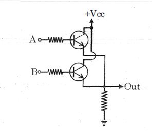
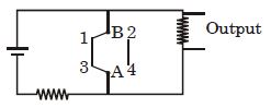
MediumMCQ
The circuit shown here can be used as a logic gate. The logic gate is
A
$AND$
B
$OR$
C
$NAND$
D
$NOR$
Solution
(B) The circuit consists of two $NPN$ transistors connected in parallel. The collectors are connected to $+V_{cc}$,and the emitters are connected together to the output terminal,which is also grounded through a resistor.
$1$. If both inputs $A$ and $B$ are at low voltage $(0)$,both transistors are in the cut-off state. The output is pulled to ground through the resistor,so $Out = 0$.
$2$. If input $A$ is high $(1)$ and $B$ is low $(0)$,the top transistor conducts,and the output voltage becomes high $(1)$.
$3$. If input $A$ is low $(0)$ and $B$ is high $(1)$,the bottom transistor conducts,and the output voltage becomes high $(1)$.
$4$. If both inputs $A$ and $B$ are high $(1)$,both transistors conduct,and the output voltage becomes high $(1)$.
The truth table is:
$A=0, B=0 \implies Out=0$
$A=1, B=0 \implies Out=1$
$A=0, B=1 \implies Out=1$
$A=1, B=1 \implies Out=1$
This truth table corresponds to the $OR$ gate.
0 likes
View Solution136
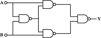
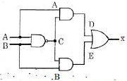
DifficultMCQ
Give the truth table for the circuit shown in the figure.
A
| $A, B, X$ |
| $0, 0, 0$ |
| $0, 1, 1$ |
| $1, 0, 1$ |
| $1, 1, 0$ |
B
| $A, B, X$ |
| $0, 0, 1$ |
| $0, 1, 0$ |
| $1, 0, 0$ |
| $1, 1, 1$ |
C
| $A, B, X$ |
| $0, 0, 0$ |
| $0, 1, 0$ |
| $1, 0, 0$ |
| $1, 1, 1$ |
D
| $A, B, X$ |
| $0, 0, 1$ |
| $0, 1, 1$ |
| $1, 0, 1$ |
| $1, 1, 0$ |
Solution
(A) Let the output of the $NAND$ gate be $C$. The boolean expression for $C$ is $C = \overline{A \cdot B}$.
Next, the top $AND$ gate takes inputs $A$ and $C$, giving output $D = A \cdot C = A \cdot (\overline{A \cdot B})$.
Similarly, the bottom $AND$ gate takes inputs $B$ and $C$, giving output $E = B \cdot C = B \cdot (\overline{A \cdot B})$.
The final output $X$ is the $OR$ of $D$ and $E$, so $X = D + E = A \cdot (\overline{A \cdot B}) + B \cdot (\overline{A \cdot B}) = (A + B) \cdot (\overline{A \cdot B})$.
Using the truth table:
This truth table corresponds to the $XOR$ gate.
Next, the top $AND$ gate takes inputs $A$ and $C$, giving output $D = A \cdot C = A \cdot (\overline{A \cdot B})$.
Similarly, the bottom $AND$ gate takes inputs $B$ and $C$, giving output $E = B \cdot C = B \cdot (\overline{A \cdot B})$.
The final output $X$ is the $OR$ of $D$ and $E$, so $X = D + E = A \cdot (\overline{A \cdot B}) + B \cdot (\overline{A \cdot B}) = (A + B) \cdot (\overline{A \cdot B})$.
Using the truth table:
| $A$ | $B$ | $C = \overline{A \cdot B}$ | $D = A \cdot C$ | $E = B \cdot C$ | $X = D + E$ |
| $0$ | $0$ | $1$ | $0$ | $0$ | $0$ |
| $0$ | $1$ | $1$ | $0$ | $1$ | $1$ |
| $1$ | $0$ | $1$ | $1$ | $0$ | $1$ |
| $1$ | $1$ | $0$ | $0$ | $0$ | $0$ |
This truth table corresponds to the $XOR$ gate.
0 likes
View Solution137
DifficultMCQ
$A$ building has two overhead water tanks, each fitted with a sensor $(S_1, S_2)$ which goes to $0$ when the water level in the tank falls below a set value and remains $1$ otherwise. $A$ common pump is used to raise water from an underground storage tank to these overhead tanks. Of the following circuits, which one will turn on $(P = 1)$ the pump only when at least one of the tanks has a water level below the set value?
A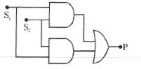
B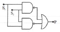
C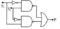
D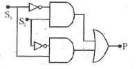
Solution
(B) The problem states that the sensor output is $0$ when the water level is below the set value, and $1$ otherwise.
We want the pump to turn on $(P = 1)$ if at least one tank has a water level below the set value.
This means $P = 1$ if $S_1 = 0$ OR $S_2 = 0$.
Using Boolean algebra, this is equivalent to $P = \overline{S_1} + \overline{S_2}$.
By De Morgan's Law, $\overline{S_1} + \overline{S_2} = \overline{S_1 \cdot S_2}$.
This is the Boolean expression for a $NAND$ gate.
Looking at the options:
Option $A$ is an $OR$ gate fed by two $AND$ gates: $P = (S_1 \cdot S_2) + (S_1 \cdot S_2) = S_1 \cdot S_2$.
Option $B$ is an $OR$ gate fed by two $NAND$ gates: $P = \overline{S_1 \cdot S_2} + \overline{S_1 \cdot S_2} = \overline{S_1 \cdot S_2}$.
This matches our requirement $P = \overline{S_1 \cdot S_2}$.
Therefore, the correct circuit is $B$.
0 likes
View Solution138
MediumMCQ
Switch $B$ can rest at either $1$ or $2$,and switch $A$ can rest at either $3$ or $4$. Determine the output expression.
A
$A \cdot \bar{B}$
B
$\overline{A \cdot B} + \bar{A} \cdot \bar{B}$
C
$A \cdot \bar{B} + B \cdot \bar{A}$
D
$\overline{A + B}$
Solution
(C) In the given circuit,the output is high only when the circuit is closed.
Let $A=0$ when switch $A$ is at $3$,and $A=1$ when switch $A$ is at $4$.
Let $B=0$ when switch $B$ is at $1$,and $B=1$ when switch $B$ is at $2$.
The circuit is closed if the path is completed. This happens when $A$ and $B$ are in different states (i.e.,one is at $1/3$ and the other is at $2/4$).
Specifically,the circuit is closed if ($A=1$ and $B=0$) or ($A=0$ and $B=1$).
This corresponds to the Boolean expression $A \cdot \bar{B} + B \cdot \bar{A}$,which is the logic for an $XOR$ gate.
0 likes
View Solution139
DifficultMCQ
The correct output for the given logic circuit and inputs is:
A
B
C
D
Solution
(D) The logic circuit consists of a $NOR$ gate followed by an $AND$ gate. The inputs to the $NOR$ gate are $A$ and $B$. The output of the $NOR$ gate is $\overline{A+B}$.
This output is then fed into an $AND$ gate along with input $B$. Thus,the final output $C$ is given by:
$C = (\overline{A+B}) \cdot B$
Let's analyze the truth table for this expression:
If $A=0, B=0$,then $C = (\overline{0+0}) \cdot 0 = 1 \cdot 0 = 0$.
If $A=1, B=0$,then $C = (\overline{1+0}) \cdot 0 = 0 \cdot 0 = 0$.
If $A=0, B=1$,then $C = (\overline{0+1}) \cdot 1 = 0 \cdot 1 = 0$.
If $A=1, B=1$,then $C = (\overline{1+1}) \cdot 1 = 0 \cdot 1 = 0$.
Wait,let's re-examine the circuit diagram. The input $B$ is connected to both the $NOR$ gate and the $AND$ gate. The output of the $NOR$ gate is $\overline{A+B}$. The $AND$ gate takes this and $B$ as inputs. So $C = (\overline{A+B}) \cdot B$. Since $(\overline{A+B}) \cdot B = (\overline{A} \cdot \overline{B}) \cdot B = \overline{A} \cdot (\overline{B} \cdot B) = \overline{A} \cdot 0 = 0$,the output is always $0$.
0 likes
View Solution140
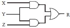
MediumMCQ
The figure shows $2$ $NAND$ gates followed by a $NOR$ gate. The system is equivalent to one gate $G$ with inputs $X, Y, Z$ and output $R$. What is $G$?
A
$OR$
B
$NAND$
C
$XOR$
D
$AND$
Solution
(D) The circuit consists of two $NAND$ gates whose outputs are fed into a $NOR$ gate. Let the inputs be $X, Y, Z$. The output of the first $NAND$ gate is $A = \overline{X \cdot Y}$ and the output of the second $NAND$ gate is $B = \overline{Y \cdot Z}$. These are the inputs to the $NOR$ gate,so the final output is $R = \overline{A + B} = \overline{\overline{X \cdot Y} + \overline{Y \cdot Z}}$. Using De Morgan's theorem,$R = \overline{\overline{X \cdot Y}} \cdot \overline{\overline{Y \cdot Z}} = (X \cdot Y) \cdot (Y \cdot Z) = X \cdot Y \cdot Z$. This is the Boolean expression for an $AND$ gate with three inputs. Thus,the system is equivalent to an $AND$ gate.
0 likes
View Solution141
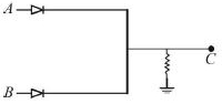
MediumMCQ
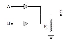
In the adjacent circuit,$A$ and $B$ represent two inputs and $C$ represents the output. The circuit represents:
A
$NOR$ gate
B
$AND$ gate
C
$NAND$ gate
D
$OR$ gate
Solution
(D) The given circuit consists of two diodes with their cathodes connected together to a common output terminal $C$,which is connected to the ground through a resistor $R_2$.
If we apply inputs $A$ and $B$ (where $0$ represents low voltage and $1$ represents high voltage),the output $C$ is determined as follows:
When both $A$ and $B$ are at $0$ (low),both diodes are reverse-biased or at the same potential,resulting in $C = 0$. If either $A$ or $B$ is at $1$ (high),the corresponding diode becomes forward-biased,pulling the output $C$ to a high state $(1)$. This truth table corresponds to an $OR$ gate.
If we apply inputs $A$ and $B$ (where $0$ represents low voltage and $1$ represents high voltage),the output $C$ is determined as follows:
| $A$ | $B$ | $C$ |
| $0$ | $0$ | $0$ |
| $0$ | $1$ | $1$ |
| $1$ | $0$ | $1$ |
| $1$ | $1$ | $1$ |
When both $A$ and $B$ are at $0$ (low),both diodes are reverse-biased or at the same potential,resulting in $C = 0$. If either $A$ or $B$ is at $1$ (high),the corresponding diode becomes forward-biased,pulling the output $C$ to a high state $(1)$. This truth table corresponds to an $OR$ gate.
0 likes
View Solution142
MediumMCQ
In the Boolean algebra,the expression $\left( {\overline {\bar A \cdot \bar B} } \right) \cdot A$ is equal to:
A
$\overline {A + B}$
B
$A$
C
$\overline {A \cdot B}$
D
$A + B$
Solution
(B) Using De Morgan's Law,$\overline {\bar A \cdot \bar B} = \overline{\bar A} + \overline{\bar B} = A + B$.
Substituting this into the expression:
$(A + B) \cdot A = A \cdot A + B \cdot A$.
Since $A \cdot A = A$,we have $A + AB$.
Factoring out $A$,we get $A(1 + B)$.
Since $(1 + B) = 1$,the expression simplifies to $A \cdot 1 = A$.
Substituting this into the expression:
$(A + B) \cdot A = A \cdot A + B \cdot A$.
Since $A \cdot A = A$,we have $A + AB$.
Factoring out $A$,we get $A(1 + B)$.
Since $(1 + B) = 1$,the expression simplifies to $A \cdot 1 = A$.
0 likes
View Solution143
DifficultMCQ
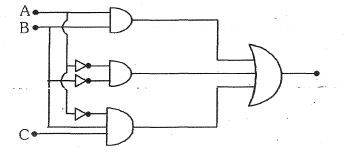
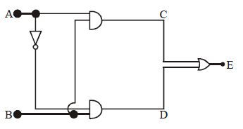
The truth table for the given logic circuit is: (Inputs $A, B$ and Output $E$)
A
| $A$ | $B$ | $E$ |
| $0$ | $0$ | $1$ |
| $0$ | $1$ | $0$ |
| $1$ | $0$ | $1$ |
| $1$ | $1$ | $0$ |
B
| $A$ | $B$ | $E$ |
| $0$ | $0$ | $1$ |
| $0$ | $1$ | $0$ |
| $1$ | $0$ | $0$ |
| $1$ | $1$ | $1$ |
C
| $A$ | $B$ | $E$ |
| $0$ | $0$ | $0$ |
| $0$ | $1$ | $1$ |
| $1$ | $0$ | $0$ |
| $1$ | $1$ | $1$ |
D
| $A$ | $B$ | $E$ |
| $0$ | $0$ | $0$ |
| $0$ | $1$ | $1$ |
| $1$ | $0$ | $1$ |
| $1$ | $1$ | $0$ |
Solution
(C) The circuit consists of two $AND$ gates and one $OR$ gate. Let the inputs be $A$ and $B$.
$1$. The upper $AND$ gate receives inputs $A$ and $B$. Its output is $C = A \cdot B$.
$2$. The lower $AND$ gate receives inputs $\bar{A}$ (from the $NOT$ gate) and $B$. Its output is $D = \bar{A} \cdot B$.
$3$. The final output $E$ is the $OR$ combination of $C$ and $D$,so $E = C + D = (A \cdot B) + (\bar{A} \cdot B)$.
$4$. Factoring out $B$,we get $E = B(A + \bar{A})$. Since $A + \bar{A} = 1$,the expression simplifies to $E = B \cdot 1 = B$.
$5$. Constructing the truth table:
- If $A=0, B=0$,then $E=0$.
- If $A=0, B=1$,then $E=1$.
- If $A=1, B=0$,then $E=0$.
- If $A=1, B=1$,then $E=1$.
This matches the truth table where $E$ is identical to $B$.
0 likes
View Solution144
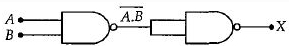
DifficultMCQ
The circuit given below is that of:
A
$AND$ gate
B
$OR$ gate
C
$NAND$ gate
D
$NOR$ gate
Solution
(C) Let the inputs be $A$ and $B$. The first gate is an $OR$ gate with one input inverted,so its output is $Y' = \bar{A} + B$.
The second gate is an $AND$ gate with inputs $Y'$,$A$,and $B$. Its output is $Y'' = Y' \cdot A \cdot B = (\bar{A} + B) \cdot A \cdot B$.
Using Boolean algebra: $Y'' = (\bar{A} \cdot A \cdot B) + (B \cdot A \cdot B) = (0 \cdot B) + (A \cdot B) = A \cdot B$.
The final gate is a $NOT$ gate,so the final output is $Y = \overline{Y''} = \overline{A \cdot B}$.
This is the Boolean expression for a $NAND$ gate.
Truth table for the circuit:
| $A$ | $B$ | $\bar{A}$ | $Y' = \bar{A} + B$ | $Y'' = Y' \cdot A \cdot B$ | $Y = \overline{Y''}$ |
| $0$ | $0$ | $1$ | $1$ | $0$ | $1$ |
| $0$ | $1$ | $1$ | $1$ | $0$ | $1$ |
| $1$ | $0$ | $0$ | $0$ | $0$ | $1$ |
| $1$ | $1$ | $0$ | $1$ | $1$ | $0$ |
0 likes
View Solution145
DifficultMCQ
The truth table for the circuit shown in the figure is
A
| $A, B$ | $Y$ |
| $1, 1$ | $1$ |
| $0, 1$ | $0$ |
| $1, 0$ | $0$ |
| $0, 0$ | $1$ |
B
| $A, B$ | $Y$ |
| $1, 1$ | $0$ |
| $0, 0$ | $1$ |
| $1, 0$ | $0$ |
| $0, 1$ | $1$ |
C
| $A, B$ | $Y$ |
| $1, 1$ | $0$ |
| $0, 1$ | $0$ |
| $1, 0$ | $0$ |
| $0, 0$ | $0$ |
D
| $A, B$ | $Y$ |
| $1, 1$ | $1$ |
| $0, 1$ | $1$ |
| $1, 0$ | $1$ |
| $0, 0$ | $1$ |
Solution
(D) The circuit consists of a $NAND$ gate and an $OR$ gate feeding into a final $OR$ gate.
Let the inputs be $A$ and $B$.
The output of the $NAND$ gate is $\overline{AB}$.
The output of the $OR$ gate is $A+B$.
The final output $Y$ is the $OR$ combination of these two: $Y = (A+B) + \overline{AB}$.
Using Boolean algebra: $Y = A + B + \bar{A} + \bar{B}$.
Since $A + \bar{A} = 1$ and $B + \bar{B} = 1$,the expression simplifies to $Y = 1 + 1 = 1$.
Thus,for all input combinations $(A, B)$,the output $Y$ is always $1$.
Therefore,the correct truth table is option $D$.
0 likes
View Solution146
EasyMCQ
The logic behind the $NOR$ gate is that it gives
A
High output when both the inputs are low
B
Low output when both the inputs are low
C
High output when both the inputs are high
D
None of these
Solution
(A) The $NOR$ gate is a combination of an $OR$ gate followed by a $NOT$ gate.
The Boolean expression for an $OR$ gate is $Y = A + B$.
The Boolean expression for a $NOR$ gate is $Y = \overline{A + B}$.
According to this expression, if both inputs $A$ and $B$ are $0$ (low), then $Y = \overline{0 + 0} = \overline{0} = 1$ (high).
If any input is $1$ (high), the output becomes $0$ (low).
Therefore, the $NOR$ gate gives a high output only when both inputs are low.
0 likes
View Solution147
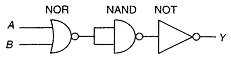
MediumMCQ
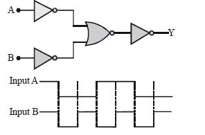
The figure shows a combination of logic gates. To what single gate is this combination equivalent?
A
$EX-NOR$
B
$NOR$
C
$EX-OR$
D
$OR$
Solution
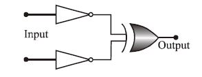
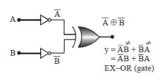
(C) Let the inputs to the two $NOT$ gates be $A$ and $B$.
The outputs of the $NOT$ gates are $\bar{A}$ and $\bar{B}$ respectively.
These outputs are fed into an $EX-OR$ gate.
The output $Y$ of the $EX-OR$ gate is given by the Boolean expression:
$Y = \bar{A} \oplus \bar{B}$
Using the property of the $EX-OR$ gate,$X \oplus Y = X\bar{Y} + \bar{X}Y$,we get:
$Y = \bar{A}(\overline{\bar{B}}) + (\overline{\bar{A}})\bar{B}$
$Y = \bar{A}B + A\bar{B}$
This is the Boolean expression for an $EX-OR$ gate.
Therefore,the given combination is equivalent to an $EX-OR$ gate.
0 likes
View Solution148
DifficultMCQ
In the circuit shown in the following figure,the value of $y$ is:
A
$0$
B
$1$
C
Fluctuates between $0$ and $1$
D
Indeterminate as the circuit cannot be realized
Solution
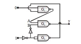
(A) Let the output of the circuit be $y$. The circuit consists of three $NAND$ gates $(G_1, G_2, G_3)$ and two $NOT$ gates.
$1$. The input to the first $NOT$ gate is $1$,so its output is $0$. This $0$ is fed to the second $NOT$ gate,making its output $1$. Thus,the input $B$ to gate $G_2$ is $1$.
$2$. The input to gate $G_3$ is $0$ (from the first $NOT$ gate) and $y$ (feedback from the output). The output of $G_3$ is $\overline{0 \cdot y} = \overline{0} = 1$.
$3$. The gate $G_1$ has inputs $0$ and $y$. Its output is $\overline{0 \cdot y} = \overline{0} = 1$. This output $1$ is the input $A$ to gate $G_2$.
$4$. Now,gate $G_2$ has inputs $A = 1$ and $B = 1$. Its output is $y = \overline{A \cdot B} = \overline{1 \cdot 1} = \overline{1} = 0$.
$5$. Since the output $y$ is $0$,the circuit is consistent. Therefore,the value of $y$ is $0$.
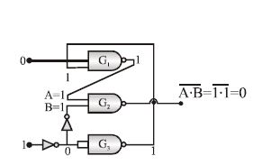
0 likes
View Solution149
MediumMCQ
Two inputs of a $NAND$ gate are shorted. This gate is equivalent to
A
$OR$ gate
B
$NOR$ gate
C
$NOT$ gate
D
$AND$ gate
Solution
(C) $NAND$ gate performs the operation $Y = \overline{A \cdot B}$.
If the two inputs $A$ and $B$ are shorted, then $A = B = X$.
Substituting this into the $NAND$ expression, we get $Y = \overline{X \cdot X}$.
Since $X \cdot X = X$, the expression becomes $Y = \overline{X}$.
This is the Boolean expression for a $NOT$ gate.
Therefore, a $NAND$ gate with shorted inputs acts as a $NOT$ gate.
0 likes
View Solution150
MediumMCQ
The truth table for the following logic circuit is:
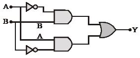
A
| $A$ | $B$ | $Y$ |
| $0$ | $0$ | $0$ |
| $0$ | $1$ | $1$ |
| $1$ | $0$ | $1$ |
| $1$ | $1$ | $0$ |
B
| $A$ | $B$ | $Y$ |
| $0$ | $0$ | $0$ |
| $0$ | $1$ | $1$ |
| $1$ | $0$ | $1$ |
| $1$ | $1$ | $1$ |
C
| $A$ | $B$ | $Y$ |
| $0$ | $0$ | $1$ |
| $0$ | $1$ | $0$ |
| $1$ | $0$ | $1$ |
| $1$ | $1$ | $0$ |
D
| $A$ | $B$ | $Y$ |
| $0$ | $0$ | $1$ |
| $0$ | $1$ | $1$ |
| $1$ | $0$ | $0$ |
| $1$ | $1$ | $1$ |
Solution
(A) The given logic circuit consists of two $NOT$ gates,two $AND$ gates,and one $OR$ gate. The output expression is derived as follows:
$1$. The upper branch gives the output $\overline{A} \cdot B$.
$2$. The lower branch gives the output $A \cdot \overline{B}$.
$3$. The final $OR$ gate combines these to give $Y = \overline{A}B + A\overline{B}$,which is the Boolean expression for an $XOR$ gate.
The truth table is:
$1$. The upper branch gives the output $\overline{A} \cdot B$.
$2$. The lower branch gives the output $A \cdot \overline{B}$.
$3$. The final $OR$ gate combines these to give $Y = \overline{A}B + A\overline{B}$,which is the Boolean expression for an $XOR$ gate.
The truth table is:
| $A$ | $B$ | $\overline{A}$ | $\overline{B}$ | $\overline{A} \cdot B$ | $A \cdot \overline{B}$ | $Y = \overline{A}B + A\overline{B}$ |
| $0$ | $0$ | $1$ | $1$ | $0$ | $0$ | $0$ |
| $0$ | $1$ | $1$ | $0$ | $1$ | $0$ | $1$ |
| $1$ | $0$ | $0$ | $1$ | $0$ | $1$ | $1$ |
| $1$ | $1$ | $0$ | $0$ | $0$ | $0$ | $0$ |
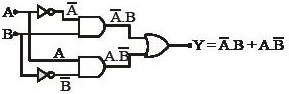
0 likes
View SolutionSemiconductor Electronics — Boolean Algebra and Logic Gates · Frequently Asked Questions
1Are these Semiconductor Electronics questions useful for JEE and NEET?
Yes. All questions in this section are mapped to JEE Main and NEET exam patterns. Previous year questions from JEE Main, NEET, GUJCET and state-level exams are included with full solutions.
2Can I switch to Hindi or Gujarati for these questions?
Yes. Use the language tabs in the hero section or the sidebar to view the same questions and solutions in English, Hindi or Gujarati.
3How do I generate a question paper from this subtopic?
Use the Vedclass Exam Paper Generator — select the chapter and subtopic, set difficulty, and generate Sets A, B, C, D automatically. First 3 chapters of every subject are free.
Vedclass Products
For Students
Vedclass Test Series
Mock tests in real JEE/NEET style with performance analysis. 5-day free trial.
Start Free TrialFor Teachers
Exam Paper Generator
Generate Set A/B/C/D papers from this chapter in 2 minutes. 3 chapters free.
Try FreeFor Institutes
Online Exam Module
Live online exams with unlimited students, 360° analytics & white-label branding.
See DemoFor Teachers & Institutes
Generate a Semiconductor Electronics Exam Paper in 2 Minutes
Select subtopic & difficulty — Sets A, B, C, D auto-generated with No Repeat logic.
First 3 chapters of every subject are free — no payment required.