
A English
Light Emitting Diode (L.E.D), Photodiode, Solar Cell Questions in English
Class 12 Physics · Semiconductor Electronics · Light Emitting Diode (L.E.D), Photodiode, Solar Cell
118+
Questions
English
Language
100%
With Solutions
Showing 50 of 118 questions in English
51
Easy
Explain why elemental semiconductors cannot be used to make visible $LEDs$.
Solution
(N/A) The band gap energy of elemental semiconductors, such as silicon $(Si)$ or germanium $(Ge)$, is relatively small. For silicon, the band gap is approximately $1.1 \text{ eV}$, and for germanium, it is about $0.67 \text{ eV}$.
Visible light corresponds to photon energies ranging from approximately $1.8 \text{ eV}$ to $3.1 \text{ eV}$.
Since the band gap of elemental semiconductors is too small, the energy released during electron-hole recombination is insufficient to produce photons in the visible spectrum. Instead, they emit radiation in the infrared region.
Therefore, compound semiconductors with larger band gaps are required to produce visible light $LEDs$.
0 likes
View Solution52
EasyMCQ
If a semiconductor photodiode can detect a photon with a maximum wavelength of $400\, nm$, then its band gap energy is (Given: Planck's constant $h = 6.63 \times 10^{-34}\, J \cdot s$, Speed of light $c = 3 \times 10^{8}\, m/s$) (in $ eV$)
A
$2.0$
B
$1.5$
C
$3.1$
D
$1.1$
Solution
(C) The band gap energy $E_g$ of a semiconductor is related to the maximum wavelength $\lambda$ of the photon it can detect by the formula: $E_g = \frac{hc}{\lambda}$.
Substituting the given values:
$h = 6.63 \times 10^{-34}\, J \cdot s$
$c = 3 \times 10^{8}\, m/s$
$\lambda = 400 \times 10^{-9}\, m$
$E_g = \frac{(6.63 \times 10^{-34}) \times (3 \times 10^{8})}{400 \times 10^{-9}}\, J$
$E_g = \frac{19.89 \times 10^{-26}}{4 \times 10^{-7}}\, J = 4.9725 \times 10^{-19}\, J$.
To convert this energy into electron-volts $(eV)$, divide by the charge of an electron $e = 1.6 \times 10^{-19}\, C$:
$E_g (in\; eV) = \frac{4.9725 \times 10^{-19}}{1.6 \times 10^{-19}} \approx 3.1\; eV$.
0 likes
View Solution53
MediumMCQ
Which of the following will $NOT$ be observed when a multimeter (operating in resistance measuring mode) probes connected across a component are reversed?
A
Multimeter shows $NO$ deflection in both cases i.e. before and after reversing the probes if the chosen component is a capacitor.
B
Multimeter shows a deflection, accompanied by a splash of light out of the connected component in one direction and $NO$ deflection on reversing the probes if the chosen component is an $LED$.
C
Multimeter shows $NO$ deflection in both cases i.e. before and after reversing the probes if the chosen component is a metal wire.
D
Multimeter shows an equal deflection in both cases i.e. before and after reversing the probes if the chosen component is a resistor.
Solution
(B) multimeter in resistance mode applies a small $DC$ voltage across the component to measure current.
$(1)$ For a capacitor, the multimeter will show a transient deflection as it charges, regardless of probe polarity. Thus, the statement that it shows $NO$ deflection is incorrect.
$(2)$ An $LED$ is a diode. In forward bias, it conducts (showing deflection), and in reverse bias, it blocks current (no deflection). The option suggests the opposite behavior, making it the observation that will $NOT$ occur.
$(3)$ For a metal wire, the resistance is nearly $0 \ \Omega$, so the multimeter will show $NO$ deflection (or a reading of $0$).
$(4)$ $A$ resistor is an ohmic component; its resistance is independent of the direction of current, so the deflection remains the same when probes are reversed.
0 likes
View Solution54
MediumMCQ
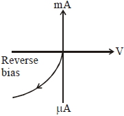
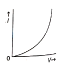
With increasing biasing voltage of a photodiode,the photocurrent magnitude
A
increases initially and saturates finally
B
increases initially and after attaining certain value,it decreases
C
increases linearly
D
remains constant
Solution
(A) photodiode is operated in reverse bias mode. When light of energy greater than the bandgap energy falls on the photodiode,electron-hole pairs are generated in the depletion region.
As the reverse biasing voltage is increased,the electric field in the depletion region increases,which helps in sweeping the generated charge carriers across the junction more effectively,thereby increasing the photocurrent.
However,once all the generated charge carriers are collected,further increase in the reverse bias voltage does not increase the photocurrent significantly,and it reaches a saturation value. This is shown in the $I-V$ characteristic curve of a photodiode.
0 likes
View Solution55
MediumMCQ
$LED$ is constructed from $GaAsP$ semiconducting material. The energy gap of this $LED$ is $1.9\, eV$. Calculate the wavelength of light emitted and its colour.
$[h = 6.63 \times 10^{-34} \, Js$ and $c = 3 \times 10^{8} \, ms^{-1}]$
$[h = 6.63 \times 10^{-34} \, Js$ and $c = 3 \times 10^{8} \, ms^{-1}]$
A
$1046\, nm$ and red colour
B
$654\, nm$ and orange colour
C
$1046\, nm$ and blue colour
D
$654\, nm$ and red colour
Solution
(D) The energy gap $E_g$ is given as $1.9\, eV$.
To convert this into Joules,we multiply by $1.6 \times 10^{-19} \, J/eV$:
$E = 1.9 \times 1.6 \times 10^{-19} \, J = 3.04 \times 10^{-19} \, J$.
The wavelength $\lambda$ is given by the formula $\lambda = \frac{hc}{E}$.
Substituting the values: $\lambda = \frac{6.63 \times 10^{-34} \times 3 \times 10^{8}}{3.04 \times 10^{-19}}$.
$\lambda = \frac{19.89 \times 10^{-26}}{3.04 \times 10^{-19}} \approx 6.54 \times 10^{-7} \, m$.
$\lambda = 654 \, nm$.
$A$ wavelength of $654 \, nm$ corresponds to the red region of the visible spectrum.
0 likes
View Solution56
MediumMCQ
Consider a situation in which reverse biased current of a particular $P-N$ junction increases when it is exposed to light of wavelength $\lambda \le 621 \, nm$. During this process,enhancement in carrier concentration takes place due to the generation of hole-electron pairs. The value of the band gap is nearly (in $eV$):
A
$1$
B
$4$
C
$2$
D
$0.5$
Solution
(C) The energy of the incident photon must be at least equal to the band gap energy $(E_g)$ to generate hole-electron pairs.
The threshold wavelength $\lambda_0$ is given as $621 \, nm$.
The band gap energy is calculated using the formula:
$E_g = \frac{hc}{\lambda_0}$
Using the approximation $hc \approx 1242 \, eV \cdot nm$:
$E_g = \frac{1242 \, eV \cdot nm}{621 \, nm} = 2 \, eV$.
Therefore,the band gap is $2 \, eV$.
The threshold wavelength $\lambda_0$ is given as $621 \, nm$.
The band gap energy is calculated using the formula:
$E_g = \frac{hc}{\lambda_0}$
Using the approximation $hc \approx 1242 \, eV \cdot nm$:
$E_g = \frac{1242 \, eV \cdot nm}{621 \, nm} = 2 \, eV$.
Therefore,the band gap is $2 \, eV$.
0 likes
View Solution57
MediumMCQ
The photodiode is used to detect optical signals. These diodes are preferably operated in reverse biased mode because:
A
fractional change in majority carriers produces higher forward bias current
B
fractional change in majority carriers produces higher reverse bias current
C
fractional change in minority carriers produces higher forward bias current
D
fractional change in minority carriers produces higher reverse bias current
Solution
(D) photodiode is a $p-n$ junction diode fabricated with a transparent window to allow light to fall on the diode. When the photodiode is illuminated with light (photons with energy $h
u > E_g$),electron-hole pairs are generated due to the absorption of photons. These charge carriers are minority carriers in the depletion region. Under reverse bias,the electric field sweeps these minority carriers across the junction,creating a current. Because the reverse saturation current is highly sensitive to the generation of minority carriers,a small fractional change in the incident light intensity produces a significant,easily detectable change in the reverse bias current.
u > E_g$),electron-hole pairs are generated due to the absorption of photons. These charge carriers are minority carriers in the depletion region. Under reverse bias,the electric field sweeps these minority carriers across the junction,creating a current. Because the reverse saturation current is highly sensitive to the generation of minority carriers,a small fractional change in the incident light intensity produces a significant,easily detectable change in the reverse bias current.
0 likes
View Solution58
EasyMCQ
The energy band gap of a semiconducting material required to produce a violet (wavelength $= 4000 \, \mathring{A}$) $LED$ is $....... \, \text{eV}$. (Round off to the nearest integer).
A
$3$
B
$2$
C
$4$
D
$5$
Solution
(A) The energy of a photon emitted by an $LED$ is given by the formula $E = \frac{hc}{\lambda}$.
Given,wavelength $\lambda = 4000 \, \mathring{A} = 400 \, \text{nm}$.
Using the relation $E \approx \frac{1240}{\lambda (\text{in nm})} \, \text{eV}$:
$E = \frac{1240}{400} \, \text{eV} = 3.1 \, \text{eV}$.
Rounding off to the nearest integer,we get $3 \, \text{eV}$.
Given,wavelength $\lambda = 4000 \, \mathring{A} = 400 \, \text{nm}$.
Using the relation $E \approx \frac{1240}{\lambda (\text{in nm})} \, \text{eV}$:
$E = \frac{1240}{400} \, \text{eV} = 3.1 \, \text{eV}$.
Rounding off to the nearest integer,we get $3 \, \text{eV}$.
0 likes
View Solution59
MediumMCQ
$A$ solar cell is to be fabricated for efficient conversion of solar radiation to emf using material $A$. The solar cell is to be mechanically protected with the help of a coating using material $B$. If the band gap energy of materials $A$ and $B$ are $E_{A}$ and $E_{B}$ respectively,then which of the following choices is optimum for better performance of the solar cell?
A
$E_{A}=1.5 \, eV, E_{B}=5 \, eV$
B
$E_{A}=1.5 \, eV, E_{B}=1.5 \, eV$
C
$E_{A}=3 \, eV, E_{B}=1.5 \, eV$
D
$E_{A}=0.5 \, eV, E_{B}=5 \, eV$
Solution
(A) For a solar cell,the material $A$ must be able to absorb a significant portion of the solar spectrum. The band gap energy of $A$ should be around $1.5 \, eV$ to efficiently convert solar radiation into electrical energy (emf).
Material $B$ is used as a protective coating. To ensure that solar radiation passes through this coating without being absorbed,the band gap energy $E_{B}$ of material $B$ must be significantly larger than the energy of the incident photons. Therefore,a large band gap like $E_{B} = 5 \, eV$ is ideal for material $B$ to remain transparent to the solar spectrum.
Thus,the optimum choice is $E_{A} = 1.5 \, eV$ and $E_{B} = 5 \, eV$.
0 likes
View Solution60
DifficultMCQ
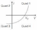
When light shines on a $p-n$ junction diode,the current $I$ versus voltage $V$ is observed as in the figure below. In which quadrant$(s)$ does the diode generate power,so that it can be used as a solar cell?
A
Quad $1$ only
B
Quad $1$ and $3$ only
C
Quad $4$ only
D
Quad $1$ and $4$ only
Solution
(C) In a solar cell,when light with energy $hf > E_g$ falls on the $p-n$ junction,electron-hole pairs are generated. These charge carriers are separated by the junction electric field,with electrons moving to the $n$-side and holes moving to the $p$-side.
If no load is connected,these charges accumulate on the $n$ and $p$ sides,creating a photo-voltage.
When an external load is connected,a photo-current $I_L$ flows through the circuit. In this state,the device acts as a power source,delivering power to the external load. The $V-I$ characteristic curve for this operation lies in the fourth quadrant,where the voltage $V$ is positive and the current $I$ is negative (indicating current flowing out of the device). Therefore,the diode generates power in the fourth quadrant.
0 likes
View Solution61
EasyMCQ
The material suitable for making a solar cell is
A
$PbS$
B
$GaAs$
C
$CdSe$
D
$Ge$
Solution
(B) The correct option is $B$.
Solar cells are devices that convert solar energy into electrical energy. The efficiency of a solar cell depends on the band gap of the semiconductor material used.
$GaAs$ (Gallium Arsenide) has a band gap of approximately $1.43 \,eV$ to $1.5 \,eV$. This value is very close to the peak intensity of the solar radiation spectrum,which makes it an ideal material for absorbing solar energy efficiently.
While $Ge$ (Germanium) and other materials are semiconductors,$GaAs$ is specifically preferred for high-efficiency solar cells due to its optimal band gap alignment with the solar spectrum.
0 likes
View Solution62
EasyMCQ
$A$ $p-n$ photodiode is manufactured from a semiconductor with a band gap of $3.1 \,eV$. Which of the following wavelengths can be detected by it?
A
$4000 \,\mathring{A}$
B
$3900 \,\mathring{A}$
C
$4200 \,\mathring{A}$
D
Both $(a)$ and $(b)$
Solution
(D) The energy of a photon is given by $E = \frac{hc}{\lambda}$.
For a photodiode to detect light,the energy of the incident photon must be greater than or equal to the band gap energy $(E_g)$ of the semiconductor.
Given $E_g = 3.1 \,eV$.
Using the relation $E \approx \frac{12400}{\lambda (\text{in } \mathring{A})} \,eV$,we set the condition $\frac{12400}{\lambda} > 3.1$.
Solving for $\lambda$,we get $\lambda < \frac{12400}{3.1} \,\mathring{A} = 4000 \,\mathring{A}$.
Since both $4000 \,\mathring{A}$ and $3900 \,\mathring{A}$ satisfy the condition $\lambda \leq 4000 \,\mathring{A}$,both wavelengths can be detected.
0 likes
View Solution63
EasyMCQ
In a $p-n$ junction solar cell,the value of photo-electromotive force produced by monochromatic light is proportional to the
A
Voltage applied at the $p-n$ junction
B
Barrier voltage at the $p-n$ junction
C
Intensity of light falling on the cell
D
Frequency of light falling on the cell
Solution
(C) In a $p-n$ junction solar cell,when monochromatic light falls on the junction,electron-hole pairs are generated due to the absorption of photons.
These charge carriers are separated by the electric field of the depletion region,creating a potential difference known as the photo-electromotive force (photo-$EMF$).
The number of electron-hole pairs generated is directly proportional to the number of incident photons per unit area per unit time,which is defined as the intensity of the light.
Therefore,the photo-$EMF$ produced is directly proportional to the intensity of the light falling on the cell.
0 likes
View Solution64
MediumMCQ
Given below are two statements: one is labelled as Assertion $A$ and the other is labelled as Reason $R$.
Assertion $A$: Photodiodes are preferably operated in reverse bias condition for light intensity measurement.
Reason $R$: The current in the forward bias is more than the current in the reverse bias for a $p-n$ junction diode.
In the light of the above statements,choose the correct answer from the options given below:
A
$A$ is false but $R$ is true.
B
Both $A$ and $R$ are true but $R$ is $NOT$ the correct explanation of $A$.
C
$A$ is true but $R$ is false.
D
Both $A$ and $R$ are true and $R$ is the correct explanation of $A$.
Solution
(B) Assertion $A$ is true: Photodiodes are designed to operate in reverse bias. In reverse bias,the reverse saturation current is very small and is highly sensitive to the incident light intensity. This makes it easier to detect small changes in light intensity.
Reason $R$ is true: For a $p-n$ junction diode,the forward bias current is significantly higher than the reverse bias current because the barrier height is reduced in forward bias,allowing majority carriers to flow easily.
However,Reason $R$ is $NOT$ the correct explanation for Assertion $A$. The reason why photodiodes are operated in reverse bias is because the fractional change in the reverse current due to incident light is much larger and easier to measure compared to the forward current,not simply because forward current is larger than reverse current.
0 likes
View Solution65
MediumMCQ
Given below are two statements: one is labeled as Assertion $A$ and the other is labeled as Reason $R$.
Assertion $A:$ Photodiodes are used in forward bias usually for measuring the light intensity.
Reason $R:$ For a $p-n$ junction diode, at applied voltage $V$, the current in the forward bias is more than the current in the reverse bias for $|V_z| > |V| \geq V_0$, where $V_0$ is the threshold voltage and $V_z$ is the breakdown voltage.
In the light of the above statements, choose the correct answer from the options given below.
A
Both $A$ and $R$ are true and $R$ is the correct explanation of $A$.
B
Both $A$ and $R$ are true but $R$ is $NOT$ the correct explanation of $A$.
C
$A$ is false but $R$ is true.
D
$A$ is true but $R$ is false.
Solution
(C) Photodiodes are specifically designed to operate under reverse bias conditions to detect light intensity, as the reverse saturation current is highly sensitive to incident light. Therefore, Assertion $A$ is false.
For a $p-n$ junction diode, the forward bias current increases exponentially with voltage once the threshold voltage $V_0$ is reached, whereas the reverse bias current remains very small until the breakdown voltage $V_z$ is reached. Thus, for the range $|V_z| > |V| \geq V_0$, the forward bias current is significantly larger than the reverse bias current. Therefore, Reason $R$ is true.
For a $p-n$ junction diode, the forward bias current increases exponentially with voltage once the threshold voltage $V_0$ is reached, whereas the reverse bias current remains very small until the breakdown voltage $V_z$ is reached. Thus, for the range $|V_z| > |V| \geq V_0$, the forward bias current is significantly larger than the reverse bias current. Therefore, Reason $R$ is true.
0 likes
View Solution66
MediumMCQ
Which of the following statements is not correct in the case of light emitting diodes?
A
$C$ and $D$
B
$A$
C
$C$
D
$B$
Solution
(C) light emitting diode $(LED)$ is a heavily doped $p-n$ junction diode.
It emits light only when it is forward biased,as the recombination of electrons and holes releases energy in the form of photons.
It does not emit light when reverse biased.
The energy of the emitted light $(E = h
u)$ is approximately equal to or slightly less than the energy band gap $(E_g)$ of the semiconductor material used.
Therefore,statement $C$ is incorrect.
0 likes
View Solution67
DifficultMCQ
Conductivity of a photodiode starts changing only if the wavelength of incident light is < 660 \, nm. The band gap of the photodiode is found to be $\left(\frac{x}{8}\right) eV$. The value of $x$ is: (Given, $h=6.6 \times 10^{-34} \, Js, c=3 \times 10^8 \, m/s, e=1.6 \times 10^{-19} \, C$)
A
$15$
B
$11$
C
$13$
D
$21$
Solution
(A) The energy of the incident photon corresponds to the band gap energy $E_g$ of the photodiode.
$E_g = \frac{hc}{\lambda}$
Given $\lambda = 660 \, nm = 660 \times 10^{-9} \, m$, $h = 6.6 \times 10^{-34} \, Js$, and $c = 3 \times 10^8 \, m/s$.
$E_g = \frac{6.6 \times 10^{-34} \times 3 \times 10^8}{660 \times 10^{-9}} \, J$
To convert this energy into $eV$, divide by the elementary charge $e = 1.6 \times 10^{-19} \, C$:
$E_g (in \, eV) = \frac{6.6 \times 10^{-34} \times 3 \times 10^8}{660 \times 10^{-9} \times 1.6 \times 10^{-19}} \, eV$
$E_g = \frac{19.8 \times 10^{-26}}{1056 \times 10^{-28}} \, eV = \frac{19.8 \times 100}{1056} \, eV = \frac{1980}{1056} \, eV$
Simplifying the fraction: $\frac{1980}{1056} = \frac{15}{8} \, eV$.
Comparing this with $\left(\frac{x}{8}\right) eV$, we get $x = 15$.
0 likes
View Solution68
DifficultMCQ
$A$ light emitting diode $(LED)$ is fabricated using $GaAs$ semiconducting material whose band gap is $1.42 \,eV$. The wavelength of light emitted from the $LED$ is: (in $\,nm$)
A
$650$
B
$1243$
C
$875$
D
$1400$
Solution
(C) The energy of the emitted photon is equal to the band gap energy of the semiconductor, $E_g = 1.42 \,eV$.
The relationship between the wavelength $\lambda$ and the energy $E$ is given by the formula: $\lambda = \frac{hc}{E}$.
Using the approximation $hc \approx 1240 \,eV \cdot nm$, we get:
$\lambda = \frac{1240 \,eV \cdot nm}{1.42 \,eV} \approx 873.24 \,nm$.
Rounding to the nearest given option, we get $\lambda \approx 875 \,nm$.
0 likes
View Solution69
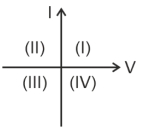
MediumMCQ
Consider the following statements $A$ and $B$ and identify the correct answer:
$A$. For a solar-cell,the $I-V$ characteristics lies in the $IV$ quadrant of the given graph.
$B$. In a reverse biased $pn$ junction diode,the current measured in $(\mu A)$ is due to majority charge carriers.
$A$. For a solar-cell,the $I-V$ characteristics lies in the $IV$ quadrant of the given graph.
$B$. In a reverse biased $pn$ junction diode,the current measured in $(\mu A)$ is due to majority charge carriers.
A
$A$ is incorrect but $B$ is correct
B
Both $A$ and $B$ are correct
C
Both $A$ and $B$ are incorrect
D
$A$ is correct but $B$ is incorrect
Solution
(D) Statement $A$: $A$ solar cell converts light energy into electrical energy. In the $I-V$ characteristic curve of a solar cell,the voltage is positive and the current is negative (as it delivers power to an external load). This corresponds to the $IV$ quadrant of the $I-V$ graph. Thus,statement $A$ is correct.
Statement $B$: In a reverse-biased $pn$ junction diode,the current is extremely small (in the order of $\mu A$) and is caused by the drift of minority charge carriers across the junction. The majority charge carriers are pushed away from the junction,preventing them from contributing to the current. Thus,statement $B$ is incorrect.
Statement $B$: In a reverse-biased $pn$ junction diode,the current is extremely small (in the order of $\mu A$) and is caused by the drift of minority charge carriers across the junction. The majority charge carriers are pushed away from the junction,preventing them from contributing to the current. Thus,statement $B$ is incorrect.
0 likes
View Solution70
MediumMCQ
Consider the following statements $:$
$A.$ The junction area of a solar cell is made very large compared to a photodiode.
$B.$ Solar cells are not connected with any external bias.
$C.$ $\text{LED}$ is made of heavily doped $p-n$ junction.
$D.$ Increase of forward current results in continuous increase of $\text{LED}$ light intensity up to a saturation point.
$E.$ $\text{LED}$ must be connected in forward bias for the emission of light.
Which of the following statements are correct?
A
$B, D, E$ Only
B
$A, C$ Only
C
$A, C, E$ Only
D
$B, E$ Only
Solution
(D) Statement $A$ is incorrect because the junction area of a solar cell is made large to collect more light,whereas a photodiode has a small area for fast response.
Statement $B$ is correct because a solar cell operates in the photovoltaic mode without any external bias.
Statement $C$ is incorrect because an $\text{LED}$ is made of a heavily doped $p-n$ junction to facilitate efficient carrier injection.
Statement $D$ is incorrect because the light intensity of an $\text{LED}$ increases with forward current only up to a certain limit,after which it saturates.
Statement $E$ is correct because an $\text{LED}$ emits light only when it is forward-biased,which causes the recombination of electrons and holes at the junction.
Therefore,statements $B$ and $E$ are correct.
0 likes
View Solution71
EasyMCQ
With increasing biasing voltage of a photodiode,the magnitude of photoelectric current
A
Remains constant
B
From photodiode in reverse bias,is zero
C
Increases initially and then saturates
D
Increases linearly
Solution
(C) photodiode is operated in reverse bias. When light of sufficient energy is incident on the photodiode,electron-hole pairs are generated in the depletion region.
As the reverse biasing voltage increases,the electric field in the depletion region increases,which helps in sweeping the generated charge carriers across the junction more effectively.
Initially,the photoelectric current increases with the increase in reverse bias voltage.
However,once the voltage is sufficient to collect all the generated charge carriers,the current reaches a saturation value and does not increase further with a further increase in the biasing voltage. This is shown in the characteristic curves for different light intensities $I_1$ and $I_2$.
0 likes
View Solution72
EasyMCQ
Assertion: $A$ $P-N$ junction diode is used in reverse bias to detect the intensity of light.
Reason: In reverse bias condition,current is small but it is more sensitive to changes in intensity of incident light.
Reason: In reverse bias condition,current is small but it is more sensitive to changes in intensity of incident light.
A
Both Assertion & Reason are True & the Reason is a correct explanation of the Assertion.
B
Both Assertion & Reason are True but Reason is not a correct explanation of the Assertion.
C
Assertion is True but the Reason is False.
D
Both Assertion & Reason are False.
Solution
(A) photodiode is a special type of $P-N$ junction diode that is operated under reverse bias conditions.
When light of energy $h\nu > E_g$ is incident on the junction,electron-hole pairs are generated.
In reverse bias,the electric field at the junction is strong,which sweeps the generated charge carriers across the junction,creating a photocurrent.
The magnitude of this photocurrent is directly proportional to the intensity of the incident light.
Even though the reverse saturation current is very small,it is highly sensitive to the intensity of incident light,making it an ideal device for light detection.
Therefore,both the Assertion and the Reason are true,and the Reason correctly explains the Assertion.
0 likes
View Solution73
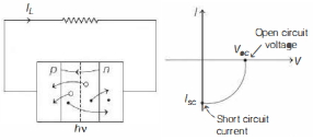
EasyMCQ
The given characteristic curve is related to which electronic device?
A
Photo diode
B
Zener diode
C
Solar cell
D
Light emitting diode $(\text{LED})$
Solution
(C) The given characteristic curve shows the $I-V$ relationship in the fourth quadrant,where the device generates power.
Specifically,it shows the 'open circuit voltage' on the $V$-axis and the 'short circuit current' on the $I$-axis.
This behavior is characteristic of a solar cell,which converts light energy into electrical energy and operates in the fourth quadrant of the $I-V$ characteristics curve.
Therefore,the correct option is $C$.
0 likes
View Solution74
MediumMCQ
For three circuit elements $A, B$ and $C$,following observations were made in lab:
$(a)$ element $A$ cannot conduct $d.c.$ but allows $a.c.$ through it.
$(b)$ element $B$ conducts both $AC$ and $DC$ but in one direction only.
$(c)$ Element $C$,when connected across $DC$,conducts only for one polarity and emits light whose intensity first increases and then decreases with increase in applied voltage.
The elements $A, B$ and $C$ are respectively identified as
A
Diode,$\text{LED}$,capacitor
B
Capacitor,diode,$\text{LED}$
C
Diode,resistor,capacitor
D
Capacitor,$\text{LED}$,diode
Solution
(B) $1$. Element $A$: $A$ capacitor acts as an open circuit for $DC$ (steady state) because its reactance $X_C = 1/(\omega C)$ is infinite at $f = 0$. However,it allows $AC$ to pass through it due to its finite reactance at non-zero frequencies.
$2$. Element $B$: $A$ diode (specifically a $p-n$ junction diode) allows current to flow only in one direction (forward bias) for both $AC$ and $DC$ signals.
$3$. Element $C$: $A$ Light Emitting Diode $(\text{LED})$ is a $p-n$ junction diode that emits light when forward-biased. The intensity of light increases with current (voltage) up to a certain point,after which it may decrease or saturate due to thermal effects or device limitations.
Therefore,$A$ is a capacitor,$B$ is a diode,and $C$ is an $\text{LED}$.
0 likes
View Solution75
MediumMCQ
The $I-V$ characteristic of an $\text{LED}$ is $:$
A
B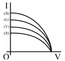
C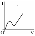
D
Solution
(A) An $\text{LED}$ (Light Emitting Diode) operates under forward bias conditions and emits light when energized.
According to the energy band theory,the energy of the emitted photon is given by $E = h\nu = \frac{hc}{\lambda} \approx E_g$,where $E_g$ is the band gap energy of the semiconductor material.
Since the frequency $\nu$ (or energy) of the emitted light is directly proportional to the band gap energy $E_g$,and the threshold voltage (potential barrier) $V_k$ is also directly related to the band gap energy $(V_k \approx E_g/e)$,it follows that light with a higher frequency requires a higher threshold voltage.
Comparing the frequencies of the colors: $\nu_{\text{blue}} > \nu_{\text{green}} > \nu_{\text{yellow}} > \nu_{\text{red}}$.
Therefore,the threshold voltage required for emission follows the order: $V_{\text{blue}} > V_{\text{green}} > V_{\text{yellow}} > V_{\text{red}}$.
This corresponds to the $I-V$ characteristic curves where the blue light curve is shifted furthest to the right along the voltage axis.
0 likes
View Solution76
EasyMCQ
$A$ $p-n$ photodiode is fabricated from a semiconductor with a band gap of $1.4 \ eV$. It can detect a signal of wavelength:
A
$8000 \ nm$
B
$8000 \ \mathring{A}$
C
$9000 \ nm$
D
$9000 \ \mathring{A}$
Solution
(B) The energy of the incident photon must be greater than or equal to the band gap energy of the semiconductor for detection to occur.
$E_{ph} \geq E_g$
Since $E_{ph} = \frac{hc}{\lambda}$,we have $\frac{hc}{\lambda} \geq E_g$,which implies $\lambda \leq \frac{hc}{E_g}$.
Using the relation $\lambda (\text{in } \mathring{A}) \approx \frac{12400}{E_g (\text{in } eV)}$,we substitute $E_g = 1.4 \ eV$:
$\lambda \leq \frac{12400}{1.4} \ \mathring{A} \approx 8857 \ \mathring{A}$.
Among the given options,the signal with a wavelength of $8000 \ \mathring{A}$ is less than $8857 \ \mathring{A}$,so it can be detected.
0 likes
View Solution77
EasyMCQ
In an $LED$,when forward bias is increased (starting from zero),the intensity of emitted light will:
A
Increase with applied bias
B
Decrease with applied bias
C
First increase and then decrease
D
Remain constant
Solution
(A) In an $LED$,the intensity of emitted light depends on the number of charge carriers crossing the junction. As the forward bias voltage increases from zero,the potential barrier decreases,allowing more electrons and holes to cross the junction and recombine. This recombination releases energy in the form of photons,thus increasing the intensity of the emitted light. Therefore,the intensity increases with the applied forward bias.
0 likes
View Solution78
MediumMCQ
The $I-V$ characteristics of an $LED$ are correctly shown by which graph?
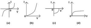
A
Graph $(a)$
B
Graph $(b)$
C
Graph $(c)$
D
Graph $(d)$
Solution
(B) An $LED$ (Light Emitting Diode) is a heavily doped $p-n$ junction diode that emits light when biased in the forward direction.
Its $I-V$ characteristics are similar to those of a standard $p-n$ junction diode.
In the forward bias region,the current increases exponentially with the applied voltage after the threshold (knee) voltage is reached.
In the reverse bias region,the current is negligible.
Graph $(a)$ represents a standard $p-n$ junction diode characteristic.
Graph $(b)$ shows a forward bias characteristic starting from the origin,which is the standard representation for an $LED$ in the first quadrant.
Therefore,graph $(b)$ is the correct representation.
0 likes
View Solution79
EasyMCQ
The $I-V$ characteristics of a photodiode for different illumination intensities $I_1, I_2, I_3$ and $I_4$ are shown in the figure. Which of the following represents the maximum intensity?
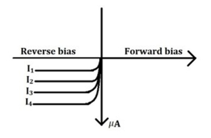
A
$I_1$
B
$I_2$
C
$I_3$
D
$I_4$
Solution
(D) photodiode is a special purpose $P-N$ junction diode fabricated with a transparent window to allow light to fall on the diode.
When the photodiode is illuminated with light,electron-hole pairs are generated due to the absorption of photons.
This results in an increase in the reverse saturation current.
The magnitude of the reverse current is directly proportional to the intensity of the incident light.
Looking at the provided $I-V$ characteristics graph,the current increases as we move from $I_1$ to $I_4$ in the reverse bias region.
Since the reverse current is highest for the curve labeled $I_4$,it corresponds to the maximum illumination intensity.
Therefore,the correct option is $D$.
0 likes
View Solution80
EasyMCQ
Identify the mismatch out of the following.
A
Zener diode - voltage regulator.
B
Photodiode - optocouplers.
C
Solar cell - Electrical energy into light.
D
Light emitting diode - optical communication.
Solution
(C) solar cell is a $P-N$ junction device that converts light energy into electrical energy. Option $C$ states that it converts electrical energy into light,which is incorrect. Therefore,it is the mismatch.
0 likes
View Solution81
EasyMCQ
Identify the correct circuit diagrams for the normal operation from the following.
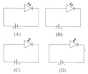
A
$(A), (B)$
B
$(B), (C)$
C
$(A), (C)$
D
$(B), (D)$
Solution
(D) photodiode is operated under reverse bias conditions. In circuit $(B)$,the $p$-side is connected to the negative terminal and the $n$-side to the positive terminal,which is reverse bias. Thus,$(B)$ is correct for a photodiode.
An $LED$ (Light Emitting Diode) is operated under forward bias conditions. In circuit $(D)$,the $p$-side is connected to the positive terminal and the $n$-side to the negative terminal,which is forward bias. Thus,$(D)$ is correct for an $LED$.
Therefore,the correct circuit diagrams for normal operation are $(B)$ and $(D)$.
0 likes
View Solution82
EasyMCQ
The following graph represents:
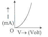
A
forward bias characteristics of a solar cell
B
reverse bias characteristics of a Zener diode
C
reverse bias characteristics of a photodiode
D
forward bias characteristics of a $LED$
Solution
(D) The graph shows current $I$ in $mA$ on the $y$-axis and voltage $V$ in $Volt$ on the $x$-axis in the first quadrant,indicating forward bias characteristics.
Among the given options,a Light Emitting Diode $(LED)$ operates in forward bias,where the current increases exponentially with voltage after the threshold voltage is reached,leading to light emission due to the recombination of charge carriers.
Therefore,the graph represents the forward bias characteristics of an $LED$.
0 likes
View Solution83
MediumMCQ
$A$ $p-n$ junction photodiode is fabricated from a semiconductor with a band gap of $2.5 eV$. It can detect a signal of wavelength: (Given: Planck's constant $h = 6.6 \times 10^{-34} Js$,speed of light $c = 3 \times 10^8 m/s$,elementary charge $e = 1.6 \times 10^{-19} C$)
A
$6000 nm$
B
$6000 Å$
C
$5000 Å$
D
$4000 nm$
Solution
(C) The energy of a photon is given by $E = \frac{hc}{\lambda}$.
For a semiconductor to detect a signal,the energy of the incident photon must be greater than or equal to the band gap energy $(E_g = 2.5 eV)$.
The threshold wavelength $\lambda$ is calculated as:
$\lambda = \frac{hc}{E_g} = \frac{6.6 \times 10^{-34} \times 3 \times 10^8}{2.5 \times 1.6 \times 10^{-19}} m$
$\lambda = \frac{19.8 \times 10^{-26}}{4.0 \times 10^{-19}} m = 4.95 \times 10^{-7} m = 4950 Å$.
Using the shortcut formula: $\lambda(Å) = \frac{12400}{E(eV)} = \frac{12400}{2.5} = 4960 Å$.
Since the photodiode detects signals with energy $E \ge 2.5 eV$,the wavelength must be $\lambda \le 4960 Å$. Among the given options,$5000 Å$ is the closest threshold,but strictly speaking,the signal must be less than the threshold. Given the standard nature of this problem,$5000 Å$ is the intended answer.
0 likes
View Solution84
EasyMCQ
The $I-V$ characteristics for a junction diode are shown. The device is
A
$LED$.
B
solar cell.
C
photocell.
D
zener diode.
Solution
(C) The $I-V$ characteristics of a device operating in the fourth quadrant (where voltage is positive and current is negative,or vice versa depending on convention) represent a device that generates power rather than consuming it.
In a $photocell$,the $I-V$ characteristics are typically shown in the fourth quadrant because it acts as a source of electrical energy when illuminated.
Therefore,the correct option is $C$.
In a $photocell$,the $I-V$ characteristics are typically shown in the fourth quadrant because it acts as a source of electrical energy when illuminated.
Therefore,the correct option is $C$.
0 likes
View Solution85
EasyMCQ
The $V-I$ characteristics of an $LED$ are correctly shown by which graph?
A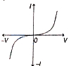
B
C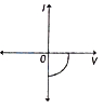
D
Solution
(B) An $LED$ (Light Emitting Diode) is a $p-n$ junction diode that emits light when it is forward-biased.
Therefore,its $V-I$ characteristics are similar to those of a standard $p-n$ junction diode operating in the forward bias region.
In the forward bias region,the current increases exponentially with the applied voltage after the threshold voltage (knee voltage) is reached.
Graph $(b)$ represents this exponential increase in current with voltage in the first quadrant,which is the characteristic behavior of an $LED$ in forward bias.
Graph $(a)$ shows both forward and reverse bias,which is for a general diode.
Graph $(c)$ represents the characteristics of a solar cell.
Graph $(d)$ represents the characteristics of a photodiode.
0 likes
View Solution86
EasyMCQ
The material used for a solar cell should have a band gap:
A
equal to zero.
B
less than $1.0 \ eV$ (non-zero).
C
more than $1.8 \ eV$.
D
between $1.0 \ eV$ and $1.8 \ eV$.
Solution
(D) solar cell is a device that converts solar energy into electrical energy. The solar radiation spectrum has a maximum intensity around $1.5 \ eV$. To efficiently absorb solar radiation,the semiconductor material used in a solar cell must have a band gap that matches this energy range. Materials with a band gap between $1.0 \ eV$ and $1.8 \ eV$ are ideal for this purpose,as they can absorb a significant portion of the solar spectrum. Silicon,with a band gap of approximately $1.1 \ eV$,is the most commonly used material for solar cells.
0 likes
View Solution87
EasyMCQ
When an $LED$ is manufactured by using aluminium gallium arsenide $(AlGaAs)$,it emits:
A
ultra-violet light
B
infra-red radiation
C
green light
D
blue light
Solution
(B) The wavelength of light emitted by an $LED$ depends on the band gap energy $(E_g)$ of the semiconductor material used.
Aluminium gallium arsenide $(AlGaAs)$ is a semiconductor material with a band gap energy that corresponds to the infra-red region of the electromagnetic spectrum.
Therefore,LEDs manufactured using $AlGaAs$ emit infra-red radiation.
Aluminium gallium arsenide $(AlGaAs)$ is a semiconductor material with a band gap energy that corresponds to the infra-red region of the electromagnetic spectrum.
Therefore,LEDs manufactured using $AlGaAs$ emit infra-red radiation.
0 likes
View Solution88
EasyMCQ
In the working of a photodiode,the reverse current depends on
A
concentration of majority carriers.
B
concentration of minority carriers.
C
applied voltage.
D
recombination of holes and electrons.
Solution
(B) photodiode is a $p-n$ junction diode operated in reverse bias.
In reverse bias,the current is primarily due to the drift of minority charge carriers across the junction.
When light (photons) with energy greater than the bandgap energy falls on the photodiode,it generates additional electron-hole pairs.
These photogenerated minority carriers are swept across the junction by the electric field,thereby increasing the reverse current.
Therefore,the reverse current in a photodiode is directly dependent on the concentration of minority carriers generated by incident light.
0 likes
View Solution89
EasyMCQ
For detecting light intensity,we use:
A
photodiode in reverse bias.
B
photodiode in forward bias.
C
$LED$ in reverse bias.
D
$LED$ in forward bias.
Solution
(A) The device used for detecting light intensity is a $Photodiode$.
$A$ $Photodiode$ is a special type of $PN$ junction diode that generates current when exposed to light.
It is specifically designed to operate in reverse biased mode.
When light falls on the junction,it creates electron-hole pairs,and the reverse current increases with the intensity of the incident light.
Therefore,it acts as a photodetector or photosensor.
0 likes
View Solution90
EasyMCQ
Which one of the following statements is $WRONG$ regarding $LED$?
A
LEDs are energy efficient.
B
LEDs have a long lifespan if properly manufactured.
C
Brightness of light emitted by $LED$ cannot be controlled.
D
Colours produced by $LED$ do not fade out.
Solution
(C) The correct answer is $C$.
$1$. LEDs are highly energy-efficient compared to conventional light sources.
$2$. LEDs have a very long operational lifespan when manufactured with high quality.
$3$. The brightness of light emitted by an $LED$ can be easily controlled by varying the forward current passing through it. Therefore,the statement that it cannot be controlled is incorrect.
$4$. The light emitted by LEDs is monochromatic and does not fade over time.
0 likes
View Solution91
EasyMCQ
For the emission of light,a light emitting diode $(LED)$ is:
A
always used in reverse biased condition
B
never used in forward or reverse biased condition
C
used both in forward and reverse biased condition depending upon its application
D
always used in forward biased condition
Solution
(D) light emitting diode $(LED)$ is a heavily doped $p-n$ junction diode which emits spontaneous radiation when forward biased.
In the forward biased condition,the potential barrier is reduced,allowing electrons from the $n$-region and holes from the $p$-region to cross the junction.
These charge carriers recombine at the junction,releasing energy in the form of photons (light).
Therefore,an $LED$ is always operated in the forward biased condition to emit light.
0 likes
View Solution92
EasyMCQ
Identify the devices which work on solar energy.
$(a)$ Photodiode
$(b)$ Photovoltaic cell
$(c)$ $LED$
$(d)$ Photo-thermal devices
$(a)$ Photodiode
$(b)$ Photovoltaic cell
$(c)$ $LED$
$(d)$ Photo-thermal devices
A
$(a)$,$(d)$
B
$(b)$,$(d)$
C
$(a)$,$(b)$
D
$(b)$,$(c)$
Solution
(B) The working principle of these devices is as follows:
$(1)$ Photovoltaic cells convert solar energy directly into electrical energy.
$(2)$ Photo-thermal devices absorb solar radiation to produce heat energy.
$(3)$ $A$ Photodiode is a light-sensitive device that generates current when exposed to light,but it is typically used as a detector rather than a primary solar energy harvester.
$(4)$ An $LED$ (Light Emitting Diode) converts electrical energy into light energy,which is the reverse of a solar cell.
Therefore,devices that primarily work on solar energy are the Photovoltaic cell and Photo-thermal devices.
0 likes
View Solution93
EasyMCQ
An $LED$ is manufactured using zinc selenide; then it emits:
A
infrared radiation
B
yellow light
C
blue light
D
green light
Solution
(C) The emission wavelength of an $LED$ depends on the band gap of the semiconductor material used. Zinc selenide $(ZnSe)$ is a wide band gap semiconductor. When an $LED$ is manufactured using zinc selenide,it emits light in the blue region of the visible spectrum.
0 likes
View Solution94
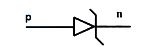
Easy
Which one of the following symbols represents a photodiode?
Solution
(D) photodiode is a special type of $p-n$ junction diode that is designed to operate under reverse bias conditions. It is sensitive to light. The symbol for a photodiode consists of a standard $p-n$ junction diode symbol with two arrows pointing towards the diode,indicating that light is incident on it. Since the provided image shows a Zener diode symbol (which has '$Z$' shaped ends on the cathode),it does not represent a photodiode. However,based on standard textbook representations,a photodiode is characterized by incoming light rays.
0 likes
View Solution95
EasyMCQ
$A$ photodiode is a device
A
in which photo current is dependent on the reverse bias.
B
which is always operated in forward bias.
C
in which photo current is independent of incident radiation.
D
which is always operated in reverse bias.
Solution
(D) photodiode is a special type of $p-n$ junction diode that is fabricated with a transparent window to allow light to fall on the diode.
It is operated under reverse bias conditions.
When light with energy $h
u$ greater than the energy gap $E_g$ of the semiconductor is incident on the diode,electron-hole pairs are generated.
Due to the electric field at the junction,these charge carriers are separated before they can recombine,resulting in a current flow in the external circuit.
The magnitude of this photo-current depends on the intensity of the incident light,not significantly on the reverse bias voltage once a certain threshold is reached.
Therefore,the correct statement is that it is always operated in reverse bias.
0 likes
View Solution96
EasyMCQ
In a light emitting diode $(LED)$,light is emitted due to:
A
drifting of electrons.
B
diffusion of holes.
C
recombination of holes and electrons.
D
emission of holes and electrons.
Solution
(C) light emitting diode $(LED)$ is a heavily doped $p-n$ junction diode.
When the diode is forward-biased,electrons from the $n$-region and holes from the $p$-region are injected into the junction region.
In the junction region,these charge carriers undergo recombination.
During the process of recombination,the energy released is in the form of photons.
If the semiconductor material has a suitable band gap,the energy of the emitted photons corresponds to the visible light spectrum.
Therefore,the light emission is due to the recombination of holes and electrons.
0 likes
View Solution97
EasyMCQ
$A$ photodiode is a device
A
which is always operated in reverse bias
B
which is always operated in forward bias
C
in which photo current is independent of intensity of incident radiation
D
which may be operated in forward or reverse bias
Solution
(A) photodiode is a semiconductor $p-n$ junction device that is specifically designed to operate under reverse bias conditions. When light of energy greater than the bandgap energy falls on the junction,it generates electron-hole pairs. The reverse bias electric field sweeps these charge carriers across the junction,creating a photocurrent that is proportional to the intensity of the incident light.
0 likes
View Solution98
EasyMCQ
The schematic symbol of a light emitting diode $(LED)$ is:
A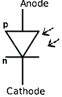
B
C
D
Solution
(B) light emitting diode $(LED)$ is a heavily doped $p-n$ junction diode which emits light when it is forward biased.
In the schematic symbol of an $LED$,the arrows point away from the diode,indicating the emission of light.
Option $A$ represents a photodiode (arrows pointing towards the diode).
Option $B$ represents an $LED$ (arrows pointing away from the diode).
Option $C$ represents a standard $p-n$ junction diode.
Option $D$ represents a Zener diode.
Therefore,the correct schematic symbol for an $LED$ is shown in option $B$.

0 likes
View Solution99
MediumMCQ
An $LED$ is a $p-n$ junction diode which is
A
forward biased
B
either forward biased or reverse biased
C
reverse biased
D
neither forward biased nor reverse biased
Solution
(A) When a $p-n$ junction diode is forward biased,the potential barrier is reduced,allowing electrons from the $n$-region and holes from the $p$-region to cross the junction.
At the junction,these charge carriers recombine,and the energy released during this process is emitted in the form of photons.
In diodes made of specific semiconductor materials like gallium arsenide or indium phosphide,this energy corresponds to the visible light spectrum.
Such a device is known as a Light Emitting Diode $(LED)$.
0 likes
View Solution100
EasyMCQ
In an $LED$,visible light is produced by:
A
Gallium phosphide
B
Gallium arsenide
C
Germanium phosphide
D
Silicon phosphide
Solution
(B) An $LED$ (Light Emitting Diode) is a heavily doped $p-n$ junction diode which emits spontaneous radiation when forward biased. The semiconductor materials used for $LEDs$ must have a band gap energy corresponding to the visible spectrum. Gallium arsenide phosphide $(GaAsP)$ or Gallium phosphide $(GaP)$ are commonly used materials. Among the given options,Gallium arsenide $(GaAs)$ is a standard semiconductor used in $LED$ technology to produce light,although its specific band gap often emits in the infrared,it is the fundamental material class used for these devices.
0 likes
View SolutionSemiconductor Electronics — Light Emitting Diode (L.E.D), Photodiode, Solar Cell · Frequently Asked Questions
1Are these Semiconductor Electronics questions useful for JEE and NEET?
Yes. All questions in this section are mapped to JEE Main and NEET exam patterns. Previous year questions from JEE Main, NEET, GUJCET and state-level exams are included with full solutions.
2Can I switch to Hindi or Gujarati for these questions?
Yes. Use the language tabs in the hero section or the sidebar to view the same questions and solutions in English, Hindi or Gujarati.
3How do I generate a question paper from this subtopic?
Use the Vedclass Exam Paper Generator — select the chapter and subtopic, set difficulty, and generate Sets A, B, C, D automatically. First 3 chapters of every subject are free.
Vedclass Products
For Students
Vedclass Test Series
Mock tests in real JEE/NEET style with performance analysis. 5-day free trial.
Start Free TrialFor Teachers
Exam Paper Generator
Generate Set A/B/C/D papers from this chapter in 2 minutes. 3 chapters free.
Try FreeFor Institutes
Online Exam Module
Live online exams with unlimited students, 360° analytics & white-label branding.
See DemoFor Teachers & Institutes
Generate a Semiconductor Electronics Exam Paper in 2 Minutes
Select subtopic & difficulty — Sets A, B, C, D auto-generated with No Repeat logic.
First 3 chapters of every subject are free — no payment required.